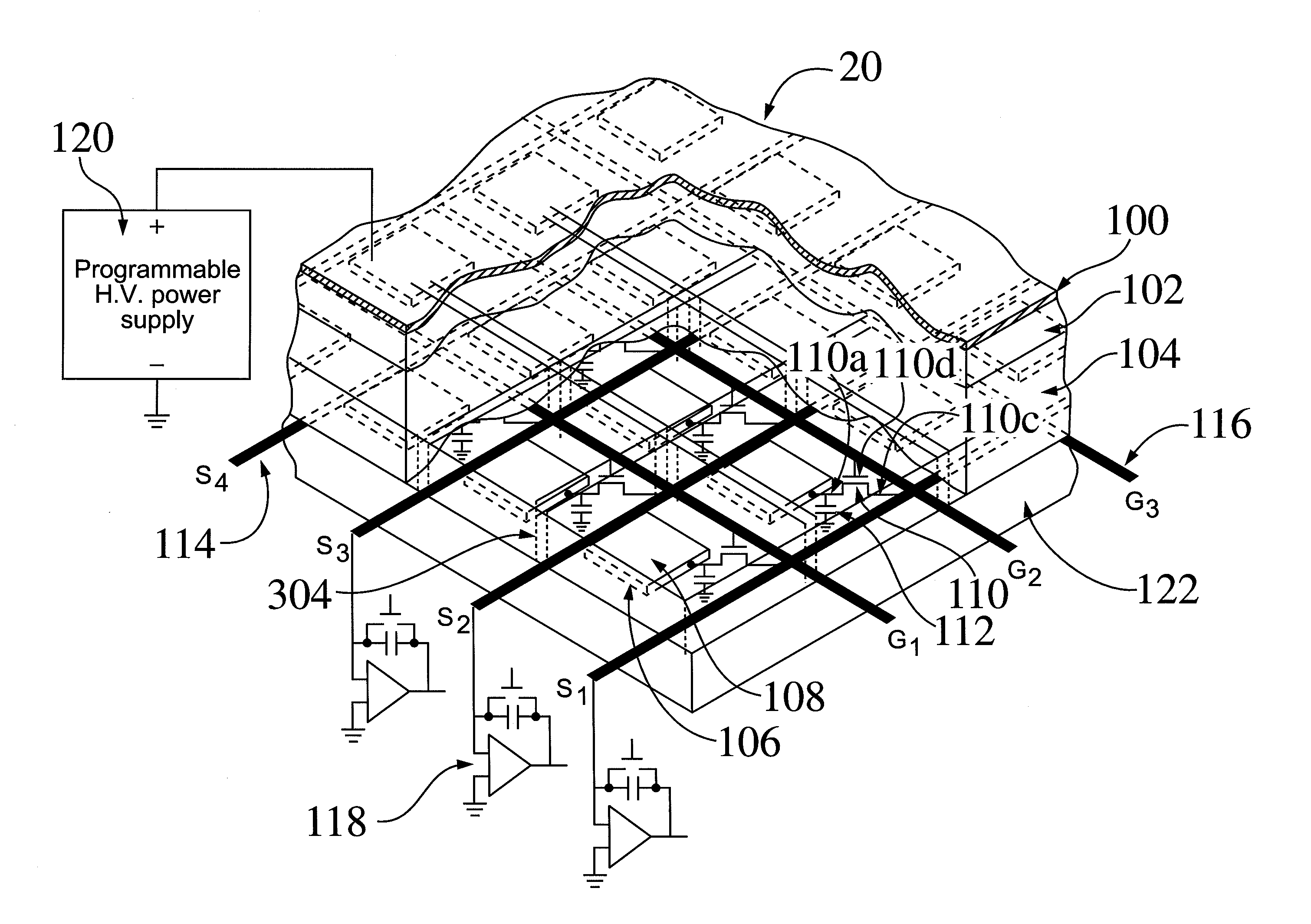
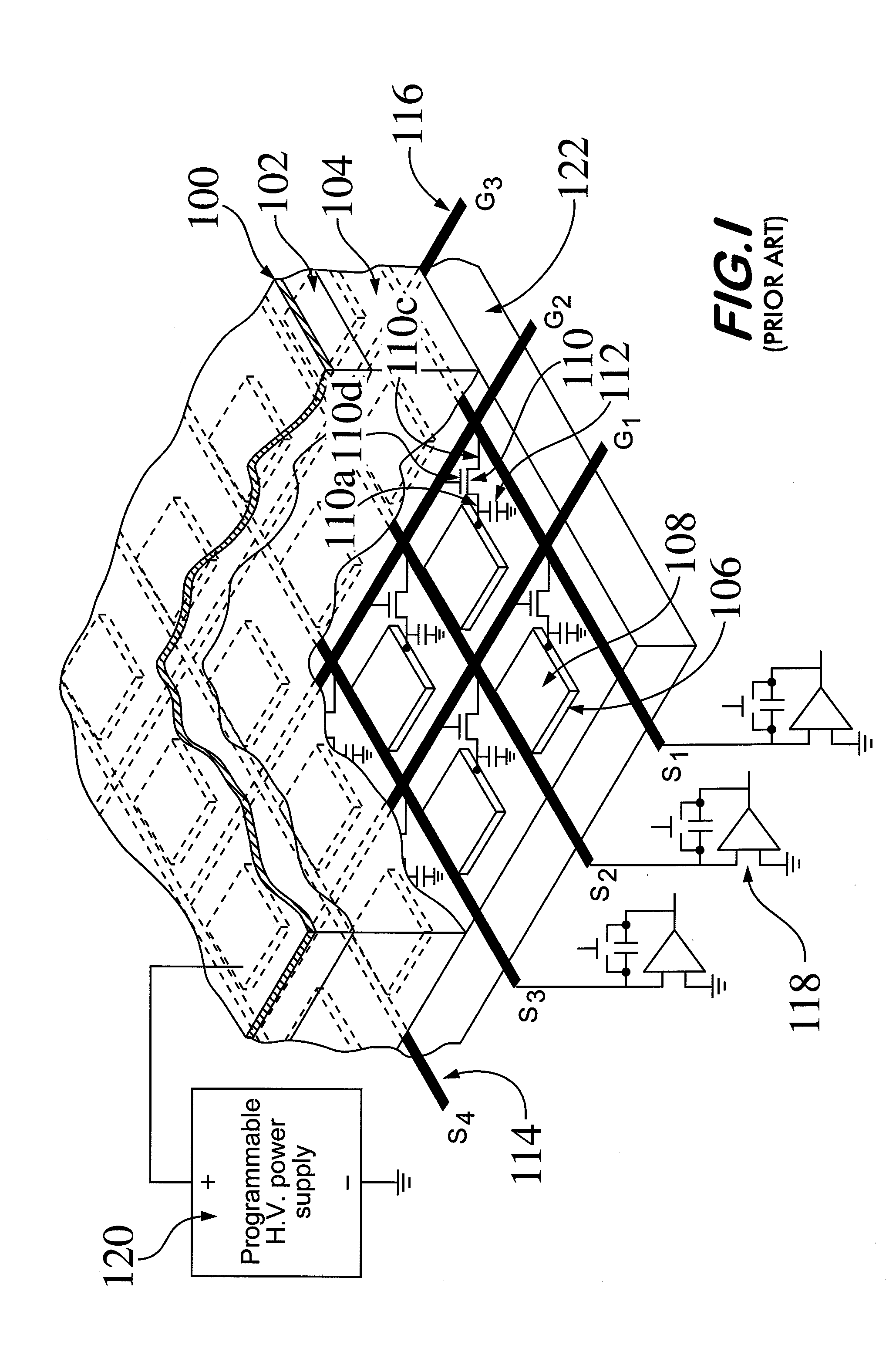
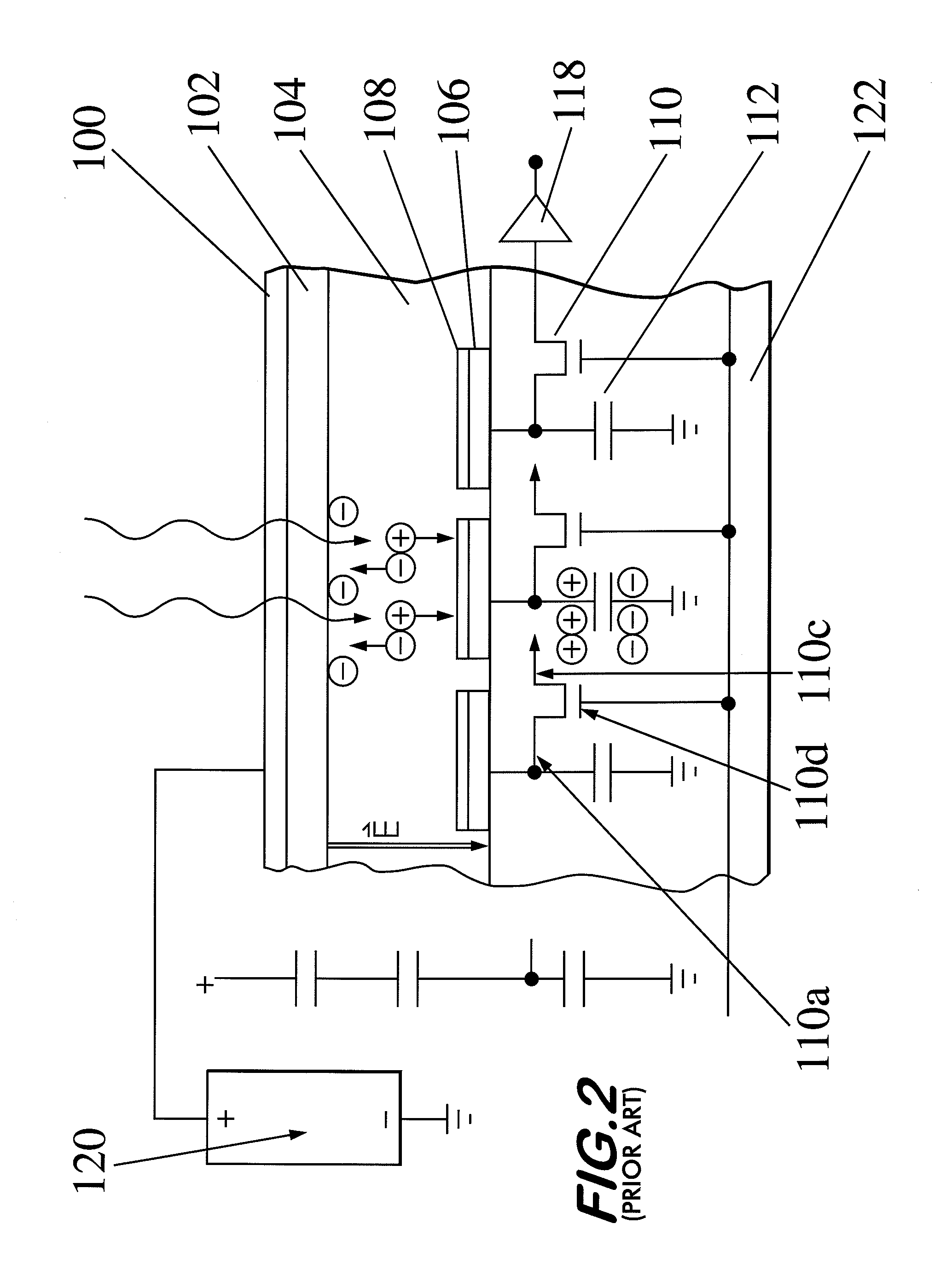
[0011]In a preferred example, a grid structure with material such as Benzocyclobutane (BCB) that can be tightly adhered to the TFT is added to the
active matrix array before the selenium layer is deposited. The ridges of this waffle like grid structure can be aligned with the gates lines and the
data lines of the underneath TFT structure to maximize the contact area of the pixel
electrode to the selenium. The typical width of these ridges is in the order of 10 micrometers or matching the width the spacing between pixels and the height of these ridges could range from 5 to 20 micrometers. This added structure changes the contacting surface of TFT to selenium from an almost flat surface to a waffle like non-flat surface. Upon changes of temperature, the elasticity of BCB and the non-flat surface with more anchoring surface area allows the contacting interfaces of selenium to remain adhered to the TFT at a lower temperature. For the high
temperature limit, these ridges also provide a barrier physically separating one pixel electrode from the next. In time, and during the gradual process of microcrystallization of amorphous selenium, these ridges provide additional electrical insulation between pixels that may be otherwise electrically bridged by the higher
conductivity of
microcrystalline selenium and resulted with
signal cross-talk between pixels or image smear. The useful life of the imaging detector can then be extended.
[0012]With the further addition of a conducting grid embedded near the top of these ridges, the x-ray
dose for a quality image can be significantly reduced by using charge multiplication effect of controlled avalanche process. This conducting grid provides an electrical potential that is just above the lower surface of the a-Se layer, and is at a
voltage level sufficient to produce a high
electric field between the grid level and the pixel electrode sufficient for avalanche charge multiplication. Because the distance between the grid and the pixel electrode is very small (e.g. about 5 to 15 μm), a practical
voltage difference across it (e.g. about 500-1500 volts) creates a sufficiently high
electric field (e.g. in the order of 100 V / μm) in the
thin layer to cause avalanche charge multiplication. The thinness of that layer which is only 1 to 3 percent of the overall selenium thickness also takes away the concerns with errors due to depth-dependent
gain. Most of the effect of converting x-ray to electrical charge occur at the 99 to 97 percent
lower field region above this bottom
high field region. The grid can be formed in using practical technology of layer and patterning that is well established in the
semiconductor industry.
[0013]As a result, lower x-ray
dose is required for the same
image quality, thus reducing
patient exposure. The lower
dose required for imaging also reduces the number of trapped charge in the bulk of the selenium charge converting layer and thus reducing the
ghosting effect known to the present in such x-ray imagers. Lower
noise and high detector
quantum efficiency (DQE) follow maintaining a high
modulation transfer function (MTF). Because the grid potential directs all or nearly all of the holes to the pixel electrodes, the
fill factor approaches 100%. Since in selenium, the threshold of
electric field for the on-set of avalanche hole multiplication is in general lower than the threshold for
electron multiplication, the charge
gain from the
avalanche effect in this structure can be limited to only the image charge of holes. Electrons injected from the TFT to selenium interface that contribute mostly to imaging
noise do not undergo charge multiplication because of the requirement of higher electric field threshold for
electron avalanche. And, the
gain factor can be conveniently adjusted from unity (no gain) to ten or more for different imaging applications simply by changing the grid potential and thus the
electrical field strength in the avalanche layer.
[0014]Two or more grids can be used, at respective
voltage levels, thus effectively providing two or more avalanche
layers with different characteristics. With two grids, the lower grid potential can be set to zero or even negative to reduce the electric field at the selenium to pixel
electrode interface and therefore reduces the electron
charge injection. The same proven
readout electronics and readout scheme used as in the current selenium
flat panel imagers commercially available, can be used in this detector with a grid structure.


