Optical pulse lasers

a laser and optical pulse technology, applied in the field of lasers, can solve the problems of incident light attenuation, incident light attenuation, and incident light attenuation, and achieve the effect of reducing the attenuation of incident light, attenuating the optical intensity of incident light, and preventing the incident light from fading

Inactive Publication Date: 2008-05-13
NAT INST OF ADVANCED IND SCI & TECH +1
View PDF43 Cites 69 Cited by
  • Summary
  • Abstract
  • Description
  • Claims
  • Application Information

AI Technical Summary

Benefits of technology

[0017]It is an object of the present invention to provide optical pulses from a mode-locked laser and / or a Q-switched laser using a saturable absorber incorporating carbon nanotubes. The optical pulse lasers of this invention use carbon nanotubes as a non-linear optical material and / or a saturable absorber for passive mode-locking and / or Q-switching, and offer several advantages over conventional materials used as saturable absorbers, such as MQW semiconductor devices. These advantages include: very fast recovery time (on the order of 1 picosecond or less), high optical damage threshold in vacuum or an inert gas environment, mechanical and environmental robustness, chemical stability, ease of fabrication, preferably at lower cost, and the ability to operate both in transmission (uni-direction), reflection and bi-directional modes. Non-linear optical carbon nanotube materials of this invention, in particular, allow the fabrication lasers with very short pulse length (on the order of 1-10 femtoseconds), similar to pulse lengths achievable using non-linear optical semiconductor materials, but which can operate in both the transmission, reflection and bi-directional modes.
[0022]In these exemplary laser configurations a wavelength coupler can be employed to couple the pump excitation beam into the gain medium. Various art-known wavelength couplers can be employed. For example, one or more optical lenses in the resonator can be employed to couple light into the saturable absorber. Optical pulses can be generated using these laser configurations by mode locking, and / or Q-switching. The carbon nanotube saturable absorber of this invention can initiate(self-start) and mode-lock a laser of various laser configurations to produce pulses ranging from picosecond-femtosecond pulses. It is believed that the intensity dependent absorption of the carbon nanotube result from the present of a limited number of exciton-absorption centers which give rise to a bleachable absorption. Further facilitating the function of these materials as saturable absorbers is the intensity dependent nonlinear phase-shift in the carbon nanotube material which gives rise to a Kerr-type nonlinear lensing effect. These effects are exploited to mode-lock a laser to produce ultra-short optical pulses.

Problems solved by technology

These optically phase-locked modes then interfere with each other to form optical pulses.
In a linear regime, where the incident optical intensity is weak, the saturable absorber absorbs the incident light, resulting in attenuation of the optical intensity of the incident light.
When the incident optical intensity is raised to a higher level, saturation of absorption occurs and absorption by the saturable absorber decreases, resulting in a decrease in attenuation of the optical intensity of the incident light.
However, not all saturable absorbers are suitable for ultra-short-pulse mode-locking application.
The saturation fluence will affect laser operating power level, which is limited by the device damage threshold.
However, a slow recovery time is also essential for self-starting of a mode-locked laser.
However, the use of dyes in laser configurations requires the use of mechanical elements such as nozzles, which are bulky and subject to mechanical malfunction and are not easily integrable with solid state lasers.
At longer wavelength in the infrared region, particular at the telecom wavelength of 1550 nm, the available dye media are easily damaged by visible light, making it more difficult to handle such materials.
MQW (multiple quantum well)semiconductor devices require complex and costly fabrication systems, such as MOCVD (metal organic chemical vapor deposition) or MOVPE (metal-organic vapor-phase epitaxy, and may require additional substrate removal process.
Furthermore, high-energy (4 MeV˜12 MeV), heavy-ion implantation is required to reduce the device recovery time (typically a few nanoseconds) to a few picosecond for laser mode-locking.
The MQW saturable absorber can only be used in reflection mode, therefore requiring inclusion of an optical circulator, which increases the total device insertion loss.
Additionally, MQW-based devices may require expensive hermetic packaging for long-tern environmental stability, and may not withstand high optical input powers.
So far, no alternative material useful as a saturable absorber at 1550 nm has been found to challenge MQW-based saturable absorbers.

Method used


Image

  • Optical pulse lasers
  • Optical pulse lasers
  • Optical pulse lasers

Examples


example 1

Preparation of Carbon Nanotubes (CNT) for Use as Non-Linear Optical and / or Saturable Absorber Materials

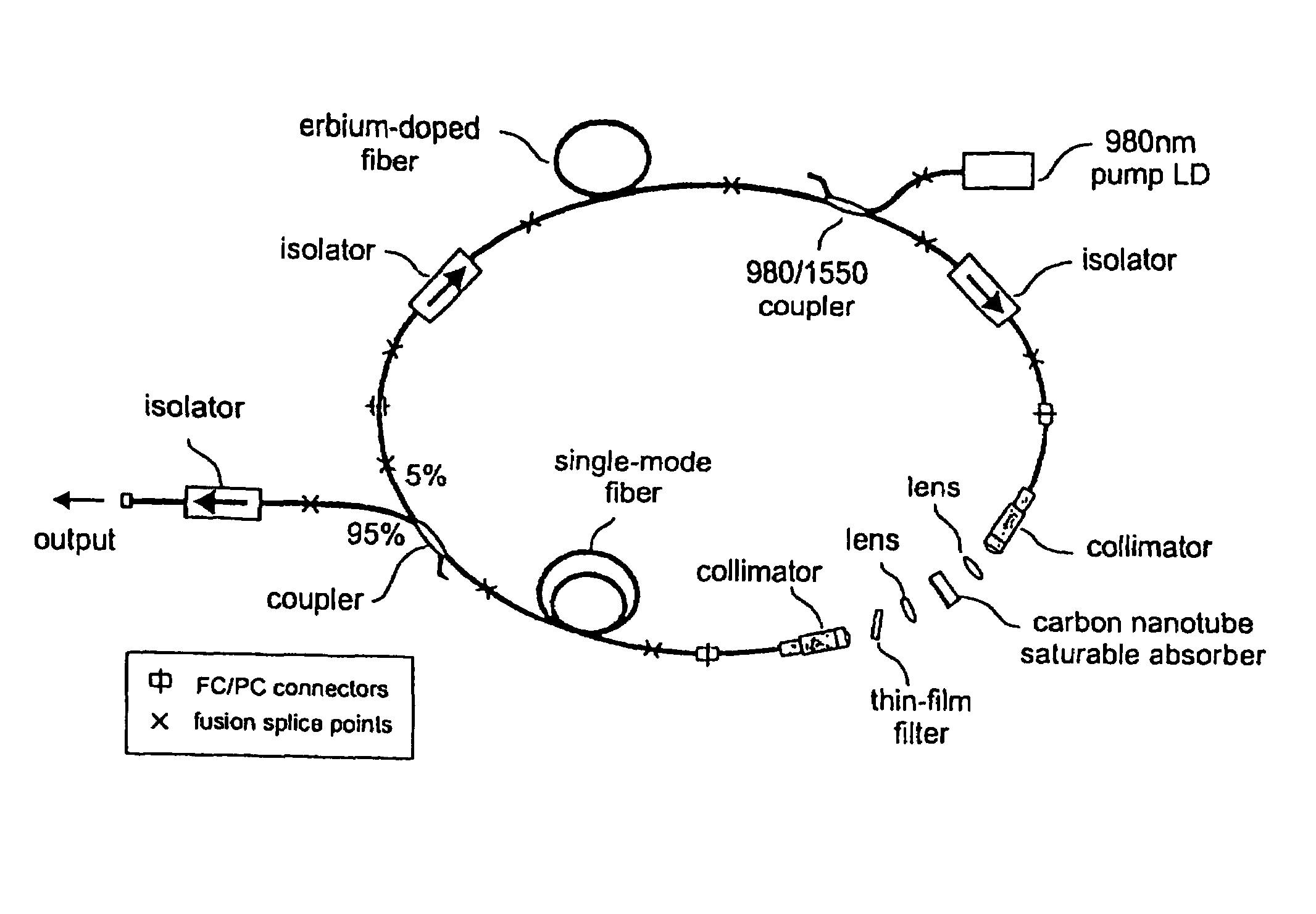
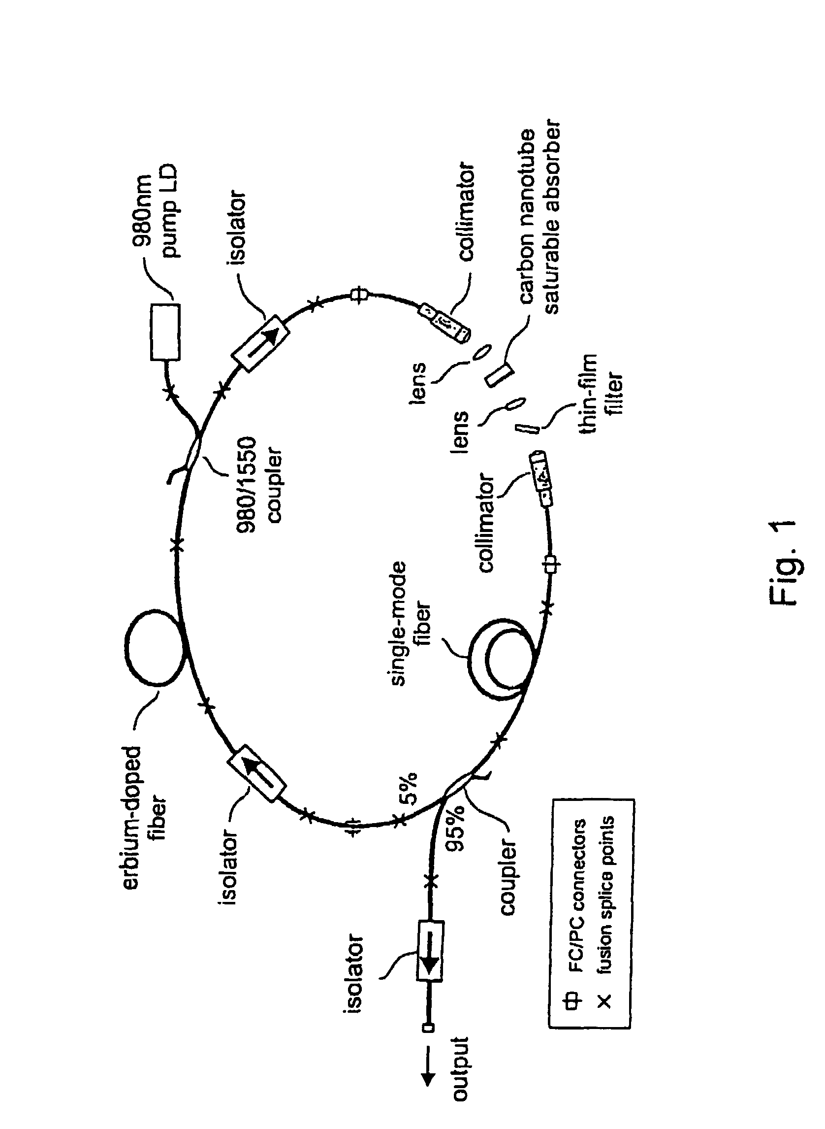
[0096]CNT can be synthesized by any means such as HiPCo, CVD, laser-oven / ablation and the arc-discharge techniques. In our particular example here, the CNT are formed by laser ablation. A target graphite rod consisting of 0.45 atomic % each of Nickel and Cobalt, placed in an oven heated at 1250° C., under 500 Torr of Argon gas flow, was ablated using the second-harmonics of a Nd:YAG pulse laser with energy of >300 mJ / pulse. At the ablated region on the carbon rod, at temperate >3000° C., the evaporated carbon atoms, assisted by the Ni / Co growth catalysts, condenses to form CNT. After laser ablation, the sample is heated (to a temperature of greater than or equal to about 120° C.) in a high vacuum to remove to vaporize substances such as fullerene with impurities. Next the sample is washed with toluene and filtered with fine mesh. Next, the sample is washed and dispersed with ethan...

example 2

Device Elements Having Layers, Films or Coatings of CNT

[0097]Various methods can be applied to obtain layers, films or coatings of CNT on substrates as illustrates in the figures herein. For example, a sample of CNT powder can be mixed with any alcohol, preferably a volatile alcohol, such as ethanol, and sprayed onto a surface.

[0098]Layers containing CNT can also be prepared by mixing the CNT powder into an adhesive or glue, such as a U-V epoxy. Preferred adhesives are those that are transparent at the intended operating wavelength or wavelengths and have a low melting point. Similarly, layers of CNT can be formed in polymers or plastics, such as polyimide. A polymer such as a polyimide can be used to form a CNT layer on or between substrates. The amount of CNT added in a layer, film or coating depends on how much absorption is desired for a given application.

[0099]CNT powders can be introduced into optical fibers. For example, CNT can be mixed into a polymer solution, which is then...


PUM

PropertyMeasurementUnit
peak poweraaaaaaaaaa
thicknessaaaaaaaaaa
telecom wavelengthaaaaaaaaaa

Abstract

The present invention provides pulsed lasers which employ carbon nanotubes, particularly layers of carbon nanotubes, as saturable absorbers, mode lockers or for Q-switching elements. The present invention also provides methods and materials for mode-locking and Q-switching of lasers in which carbon nanotubes are employed as non-linear optical materials and / or saturable absorbers which facilitate mode-locking and / or Q-switching. The invention further provides mode locker and Q-switching elements or devices which comprise one or more layers containing carbon nanotubes which layer or layers function for mode locking and / or Q-switching.

Description

CROSS-REFERENCE TO RELATED APPLICATIONS[0001]This application is a 371 national stage of PCT / US2003 / 041091, filed Dec. 22, 2003, and takes priority under 37 CFR 119(e) to U.S. provisional application Ser. No. 60 / 435,577, filed Dec. 20, 2002, both of which are incorporated by reference in their entirety herein.FIELD OF THE INVENTION[0002]The present invention is related to lasers, and more specifically, to optical pulse lasers employing nonlinear optical and / or saturable absorber elements and devices incorporating carbon nanotubes to achieve mode locking and / or Q-switching.BACKGROUND OF THE INVENTION[0003]Optical pulse lasers have great potential for applications in various fields, such as optical communications, optical signal processing, laser surgery, biomedicine, optical diagnostics, two-photon microscopy, optical probing, optical reflectometry, material processing, etc. There are two main classes of optical pulse lasers, namely mode-locked lasers and Q-switched lasers. Mode-lock...

Claims


Application Information

Patent Timeline
Patent Type & Authority Patents(United States)
IPC IPC(8): H01S3/13G02F1/35H01SH01S3/067H01S3/083H01S3/098H01S3/113
CPCB82Y10/00B82Y20/00G02B5/08G02F1/3523H01S3/06791H01S3/1118H01S3/0064H01S3/0602H01S3/0632H01S3/067H01S3/06712H01S3/08059H01S3/09415H01S3/1109H01S3/1121H01S3/113H01S3/1608
Inventor JABLONSKI, MARK KENNETHSET, SZE YUNTANAKA, YUICHI
Owner NAT INST OF ADVANCED IND SCI & TECH
Why Eureka
Try Eureka