Method and apparatus for optical signal processing using an optical tapped delay line

a delay line and optical signal technology, applied in the field of optical communication, can solve the problems of reducing the carrying capacity of fabry-perot interferometers, reducing the efficiency of optical throughput, and the relative high cost of installing new fiber optic cables, so as to reduce the size of these devices and components, reduce the cost of unit cost and the spatial requirements of otdl devices and components, and achieve significant economic advantages.

Active Publication Date: 2009-03-24
NORTHROP GRUMMAN SYST CORP
View PDF73 Cites 39 Cited by
  • Summary
  • Abstract
  • Description
  • Claims
  • Application Information

AI Technical Summary

Benefits of technology

[0120]Integrated Optics. To address the issues associated with fabricating bulk optical OTDL devices, the present invention implements the use of integrated optical packaging to manufacture the component elements of an OTDL communications device as either monolithic or hybrid planar waveguide structures. Use of well known prior art methods of producing integrated optic devices, also known as Planar Lightwave Circuits (PLC's), creates significant economic advantages in the manufacture of OTDL devices and components, as well as reducing the size of these devices and components. By reducing both the unit cost and the spatial requirements of OTDL devices and components, the cost of implementing this technology in communications networks is commensurately reduced, and the optical efficiency of the network is commensurately increased.
[0121]As described within this patent application and that of co-pending U.S. patent application Ser. No. 09 / 687,029, the Optical Tapped Delay Line (OTDL) technology is based upon the use of bulk optics to achieve extremely narrow channel spacing for various fiber optic telecommunication WDM functions. However, at its basic level, OTDL is a one-dimensional technology. Only one of the two lateral dimensions, x and y, is used for performing the optical signal processing function, in addition to the third dimension, z, which is the nominal direction of light propagation through the device. As such, fabrication of 1-D OTDL devices in monolithic or hybrid planar waveguide structures is feasible.
[0122]The fundamental methodologies for fabricating these devices exist and are currently used to fabricate several useful fiber optic telecommunications products, including arrayed waveguide (AWG) multiplexers and demultiplexers. The invention presented herein describes methods and apparatus for fabricating OTDL devices using high-resolution planar integrated optics. The fabrication of integrated optic OTDL multiplexer / demultiplexer and modulator devices affords extremely compact WDM system components with high channel counts, narrow channel spacing, and minimal part counts thereby offering substantial economic advantages over alternative technologies.
[0123]The present invention provides a high resolution integrated optical OTDL WDM device, which can be used to demultiplex an optical signal carrying multiple wavelengths of modulated data. By operating the integrated optical OTDL demultiplexer in the reverse direction, the device can function as a multiplexer to combine discrete wavelength signals into a single optical fiber output. In a third embodiment, an integrated optical OTDL demultiplexer and multiplexer are individually coupled to a data-modulator array to function as a WDM multi-channel modulator device. And in an additional embodiment, the integrated optical device features a curved, self-focusing OTDL cavity, which eliminates the need for a separate lens system to manipulate the individual beamlets emanating from the OTDL cavity output, thereby rendering a lower part count ant a smaller device footprint. Additional embodiments of the monolithic integrated optic OTDL demultiplexer / multiplexer devices are also described, in which evanescent coupling is used as an alternative means of wavelength separation of a multi-channel optical signal.

Problems solved by technology

The relatively high cost of installing new fiber optic cable presents a barrier to increased carrying capacity, however, so it is highly desirable to increase the data carrying capabilities of existing fiber.
The Fabry-Perot interferometer is not well suited for use as a WDM channelizer due to the difficulty in obtaining high optical throughput efficiency.
It is difficult to collect this light efficiently and concentrate it at multiple detector points, or couple it to multiple output fibers, especially while maintaining the separation of wavelength components that the interferometer has produced.
This fanning makes it easy to concentrate the output light at multiple detector points or fibers, but there is inherently high loss.
However, the absence of a surface coating means that it is not possible to tailor the fringe intensity profile.
This makes the Lummer-Gehrcke interferometer impractical for use in WDM applications in which the fringe profile controls the channel filter shape.
The Lummer-Gehrcke interferometer also is not well suited for use as a WDM channelizer due to the difficulty in obtaining high optical throughput efficiency.
It is difficult to collect this light efficiently and concentrate it at multiple detector points, or couple it to multiple output fibers, especially while maintaining the separation of wavelength components that the interferometer has produced.
Again, it is difficult to collect this light efficiently, and there is generally an inherent loss.
The exiting beams interfere with each other.
This overlap effect makes weighting the individual virtual sources possible only in an area-average sense, thus limiting the degree to which the channel filter shape can be tailored.
However, the line-focused input makes the VIPA impractical for fine channelization (i.e., narrow channel spacing on the order of one GHz) due to the fact that a thicker plate is needed, which would result in excessive beam divergence and overlap at the exit surface.
Since the interference filters produced by thin film coatings tend to have relatively wide passbands, they cannot achieve high resolution (twenty-five GHz or finer).
In addition, stacking thin-film filters such as the device in U.S. Pat. No. 6,111,474 produces loss that effectively limits the number of channels.
Diffraction gratings of reasonable size do not have sufficient resolution for HWDM.
They also have high optical insertion loss, making them inefficient for use in high-resolution WDM systems.
Diffraction gratings tend to produce undesirable polarization effects.
AWGs have the inherent disadvantage of a much smaller free spectral range that limits the total number of channels and increases the near-end crosstalk that affects bidirectionality.
It is difficult to achieve resolution better than fifty GHz using an AWG.
AWG devices capable of one GHz resolution would be physically large, expensive, and have very high loss.
It is important to use one grating per wavelength channel, so there is an inherent limitation on the number of channels that can be de-multiplexed with such devices due to the shear bulk of the resulting system.
A primary disadvantage of a fiber grating is that it can reflect only one wavelength.
These operations also require inflexible devices that are costly and difficult to upgrade as system capacity demand is increased.
Second, OADMs require smaller packaging because removing the electrical conversion step results in a reduced component count within the switches.
Although such filters have good channel isolation, they tend to exhibit a transmission light loss of approximately 10%.
Such filters are also highly temperature-sensitive.
Further, they often operate in only one direction.
In addition, such filters are limited to a single, fixed wavelength.
This results in increased complexity, optical loss, and cost.
The device illustrated in FIG. 6 is limited in that it can add / drop only a single wavelength.
This results in increased complexity and cost.
However, with diffraction grating systems, the component count can rise rapidly.
However, they are limited in that several fiber gratings must be combined, along with optical circulators, in order to handle a multiplexed optical signal with a high channel count.
The result can be a very large device with a high component count, increased complexity, and a higher cost.
In addition, the combination or cascading of multiple-fiber Bragg gratings can significantly reduce signal strength as the insertion loss of multiple devices is compounded throughout the system.
However, this technique is subject to very high optical component count.
Assembling and aligning these optical components within a device can be extremely expensive.
This ability is important because the optical to electrical to optical conversion process is expensive and uses significant power as well as space.
However, it is only possible to interact with a single wavelength at one time using this technique.
However, this system can only accommodate adding or dropping a single channel simultaneously.
But in practice, due to the need to maintain low cross-correlation properties between the high rate sequences, the number of usable sequences, hence users, is somewhat less than the processing gain.
The main problem with fiber optic systems is the inefficient nature of dedicated bandwidth allocation architectures.
Many communications, particularly Internet Protocol communications, are extremely bursty.
This may not be feasible.
This inherently reduces optical efficiency because a “0” code removes or discards available light.
However, detection of bi-polar codes requires detection in the presence of an unmodulated reference beam, i.e., coherent detection.
Coherent detection is difficult and expensive to achieve in a practical system.
The Dutt system is not very optically efficient due to the use of unipolar codes and it has a limited code set.
The Pfeiffer systems are more efficient but also have a limited code set resulting in a limited number of users.
This scheme cannot achieve optimal optical efficiency.
This multi-stage system is complex to build and relies on two fiber Bragg gratings.
This is less optically efficient than using a single grating.
The number of frequency bands, and hence, the number of available codes, and therefore users, is limited in a practical system.
In summary, the existing methods of OCDMA are not very efficient which yields a lower number of potential users.
Furthermore, they rely upon grating technologies that have limited resolution.
Lastly, some of the more efficient methods are complex and costly to manufacture.
In particular, maintaining increasingly narrower channel spacing demands extreme precision in the frequency stability from the source laser—a precision that is not reliably achievable.
Factors such as equipment aging, device tolerances, power source fluctuations, and temperature changes all serve to complicate the problem.
The likely result is that the frequency of interest “drifts” relative to the target or detector with a corresponding degradation of the signal.
These devices effectively solve the problem of frequency drift, but at relatively high cost and with a loss of overall efficiency due to the power requirements.
These devices vary in size, complexity and cost.
The Fabry Perot etalon does not serve well as a WDM channelizer due to the difficulty in obtaining high optical throughput efficiency.
It is difficult to collect this light efficiently and concentrate it at multiple detector points, or couple it to multiple output fibers, especially while maintaining the separation of wavelength components that the etalon has produced.
This fanning makes it easy to concentrate the output light at multiple detector points or fibers, but there is inherently high loss.
It is currently impossible to obtain such a filter in practice, but the more closely a device approximates this ideal the better its signal processing capability becomes.
Grating-based technologies are effectively limited to 50 GHz resolution.
An adverse effect of this technique is an approximate 3 dB loss in signal strength because of the abnormal shape of the resulting passband.
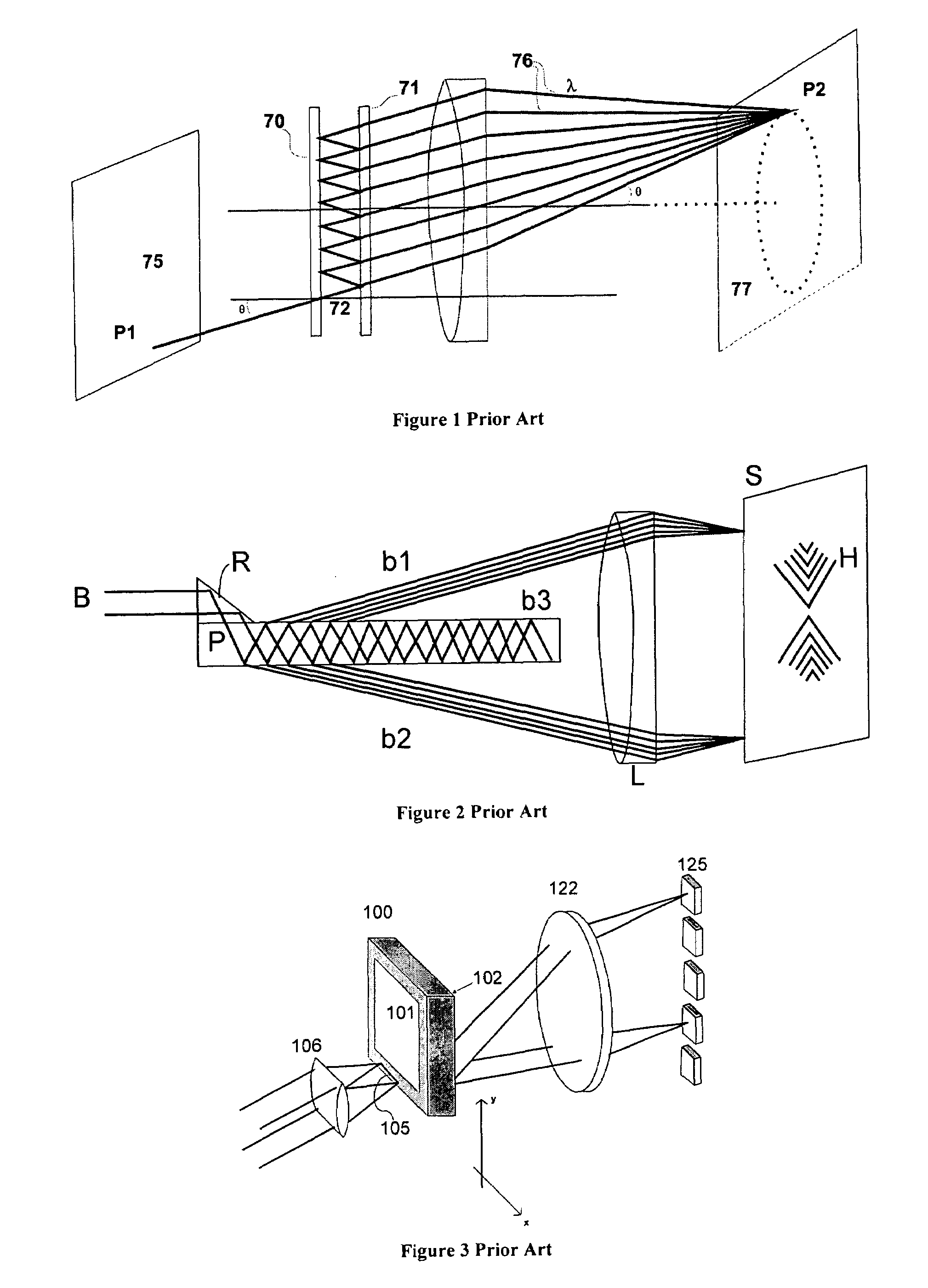
It is apparent from FIG. 9 that the prior art interleaver architecture is relatively complex and requires multiple devices, which introduces undesirable power losses into the system and increases device size and costs.
Although this can be accomplished, the size of the diffraction gratings and the expense of making such a large device creates a practical limit on the resolution of diffraction-grating based OSAs at 30 to 50 picometers.
One trend in this direction is decreasing the spacing between wavelengths to 25 GHz, 12.5 GHz and less However, as channel spacing decreases common WDM network problems such as transmitter wavelength drift, filter concatenation, and signal distortion can more easily cause cross-talk between these closely-spaced channels.
However, current WDM integrated optic technologies suffer from the same channel spacing and resolution limitations as their bulk optic counterparts.
Although integrated optical diffraction grating-based devices, such as the aforementioned examples, are being used in WDM systems, their resolution is limited.
An IO WDM device with a diffraction grating and an AWG would need to be very large and expensive to have sub-50 GHz channel resolution, and would suffer from very high loss.
However, this device cannot produce the narrow channel spacing and high channel counts of an OTDL-based integrated optical demultiplexer.
However, the fabrication of this IO demultiplexer could be extremely difficult and expensive due the precision required in the thin film deposition process to lay down the prism and lens layers, as well as the nature of the stack materials.
The drawback to this type of integrated optical WDM demultiplexer / multiplexer is the inherently high loss associated with the thin film wavelength-separation elements, which limits the number of channels that can be effectively demultiplexed, as well as the level of channel spacing within a DWDM system.
Such a method of construction could be very labor intensive and expensive as each optical component and sub-system must be aligned and fixed in place.
Maintaining important fabrication and functional tolerances can be difficult.
In today's WDM networks, this can be a disadvantage as component dimensions are crucial to system construction and cost.
Furthermore, the optical cavity technique affords a smaller package footprint than that of an AWG device performing an equivalent function.

Method used


Image

  • Method and apparatus for optical signal processing using an optical tapped delay line
  • Method and apparatus for optical signal processing using an optical tapped delay line
  • Method and apparatus for optical signal processing using an optical tapped delay line

Examples


Embodiment Construction

[0181]The following detailed description is of the best presently contemplated mode of carrying out the invention. This description is not to be taken in a limiting sense, but is made merely for the purpose of illustrating the general principles of the invention. The scope of the invention is best defined by the appended claims.

[0182]Optical Tapped Delay Line. FIGS. 11 and 12 illustrate a preferred embodiment of an OTDL device in accordance with the present invention. In the illustrated example, six collimated input beams 230a-230f enter a transparent plate 231. The origin of the beams may be, for example, the collimated outputs of six optical fibers (not shown) where each fiber typically carries multiple wavelength channels. The plate 231 has a first surface 232 that is provided with a coating 235 that is substantially 100% reflective. The plate 231 has a second surface 236 that is spaced from and opposed to the first surface 232. The second surface 236 is provided with a coating 2...


PUM


Abstract

An Optical Tapped Delay Line (OTDL), which resolves multiple wavelength signals having extremely narrow wavelength spacing, is combined with other known optical devices to provide a wide variety of optical signal processing applications, including: multiplexing and de-multiplexing a multi-channel signal; adding a signal to, or dropping a signal from, a multi-channel optical signal; specialized coding processing such as generating code division multiple access signals; wavelength locking (stabilizing) a signal; filtering a signal; and analyzing and monitoring a signal spectrum. The OTDL spatially separates individual channels to allow separate processing on each channel. Fixed and tunable embodiments are identified in appropriate cases. Bulk, hybrid, and integrated optical embodiment and methods of fabrication are described, as are curved self-focusing and evanescent embodiments of OTDL devices. The devices and processes disclosed have particular application to dense wavelength division multiplexing (DWDM) and permit a significant improvement in the quantity of information that can be carried on DWDM signals while enhancing signal quality.

Description

BACKGROUND OF THE INVENTION[0001]1. Field of the Invention[0002]The present invention relates to optical communications, and more particularly to devices and methods for manipulating a multi-frequency input signal, such as a WDM or DWDM signal, to perform a variety of optical signaling processes.[0003]2. Background of the Invention[0004]Fiber optic cable is widely used for data transmission and other telecommunication applications. The relatively high cost of installing new fiber optic cable presents a barrier to increased carrying capacity, however, so it is highly desirable to increase the data carrying capabilities of existing fiber. Wavelength division multiplexing (WDM) enables different wavelengths to be carried over a common fiber optic waveguide. WDM can separate the fiber bandwidth into multiple discrete channels through a technique referred to as dense wavelength division multiplexing (DWDM). This provides a relatively low cost and proven method of substantially increasing...

Claims


Application Information

Patent Timeline
Patent Type & Authority Patents(United States)
IPC IPC(8): H04J14/02G02B6/28G02B6/34
CPCG02B6/2861G02B6/29358H04J14/0201H04J14/021H04J14/02H04J14/0206H04J14/0208H04J14/0209H04J14/0213
Inventor TURPIN, TERRY M.PRICE, CRAIG H.FROELICH, FRED F.NICHOLS, BRUCE D.LAFUSE, JAMES L.FRAMPTON, KEITH R.
Owner NORTHROP GRUMMAN SYST CORP
Why Eureka
Try Eureka