Selective etching and formation of xenon difluoride

a technology of xenon difluoride and selective etching, which is applied in the field of electromechanical devices, can solve the problems of ion source region deposition and contamination of surfaces, defects of electronic product components, and high cost of xenon difluorid

Active Publication Date: 2012-10-02
VERSUM MATERIALS US LLC
View PDF27 Cites 12 Cited by
  • Summary
  • Abstract
  • Description
  • Claims
  • Application Information

AI Technical Summary

Benefits of technology

[0027]an ability to selectivity remove TiN films from quartz, i.e., SiO2, and SiN coated surfaces found in the cleaning of deposition chambers;
[0029]an ability to activate perfluoro etching agents in remote plasma to remove TiN films from SiO2 and SiN surfaces without adverse effects normally caused by fluorine atoms attacking in the remote plasma.

Problems solved by technology

Any material, film and the like that builds up on the walls, tool surfaces, susceptors and other equipment is considered a contaminant and may lead to defects in the electronic product component.
In the ideal case, all feedstock molecules would be ionized and extracted, but in reality a certain amount of feedstock decomposition occurs, which results in the deposition on and contamination on the surfaces in the ion source region, or parts of the ion implanter tool, such as, low voltage insulators and the high voltage components.
However, xenon difluoride is expensive, and is a material difficult to deal with.
Xenon difluoride is unstable on contact with air, light or water vapor (moisture).
Hydrogen fluoride is not only dangerous, but also reduces efficiency of etching.
Additionally, xenon difluoride is a solid having a low vapor pressure which makes deliver of xenon difluoride to the process chamber difficult.
However, the etching effect is not as efficient as the use of xenon difluoride.
Many of the conventional fluorine based etchants that attack TiN films also attack SiO2 and SiN surfaces and, therefore, unacceptable for removing TiN deposition products from semiconductor deposition chambers and equipment.

Method used


Image

  • Selective etching and formation of xenon difluoride
  • Selective etching and formation of xenon difluoride
  • Selective etching and formation of xenon difluoride

Examples


example 1

Effectiveness of XeF2 in Etching of Deposition Materials at Various Temperatures and Pressures

[0066]In this example, the etch rates for TiN, SiO2, and SiN were determined using XeF2 as the etchant at various temperatures and pressures. Experimental samples were prepared from Si wafers coated with thin films of TiN, SiO2, and SiN. Etch rates were calculated by the thin film thickness change between the initial film thickness and that thickness after a timed exposure to the etching or processing conditions.

[0067]To effect etching bulk XeF2 gas was introduced from a cylinder into the reactor chamber through an unused remote plasma generator. The XeF2 gas pressure in the reactor chamber was held constant by turning off the flow from the cylinder once the desired pressure was reached.

[0068]The test coupons were placed on the surface of a pedestal heater which was used to maintain different substrate temperatures. The results are shown in Table I below.

[0069]

TABLE IETCH RATES FOR VARIOUS ...

example 2

Selective Etching of Si to SiO2

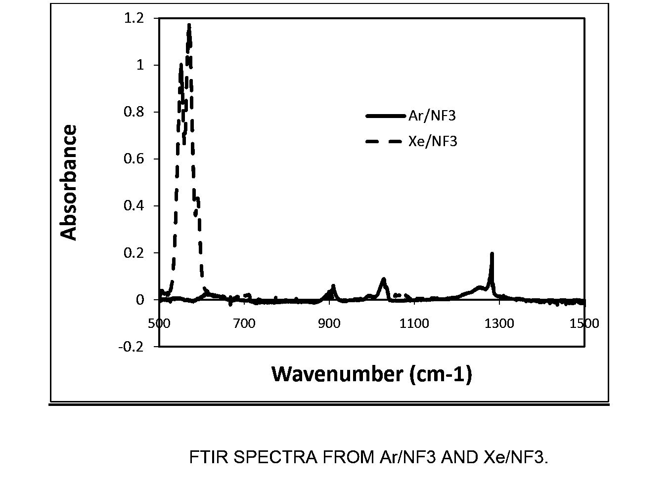
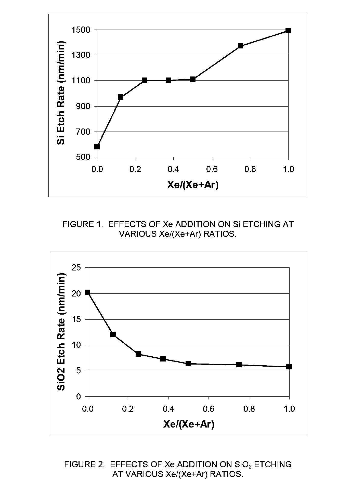
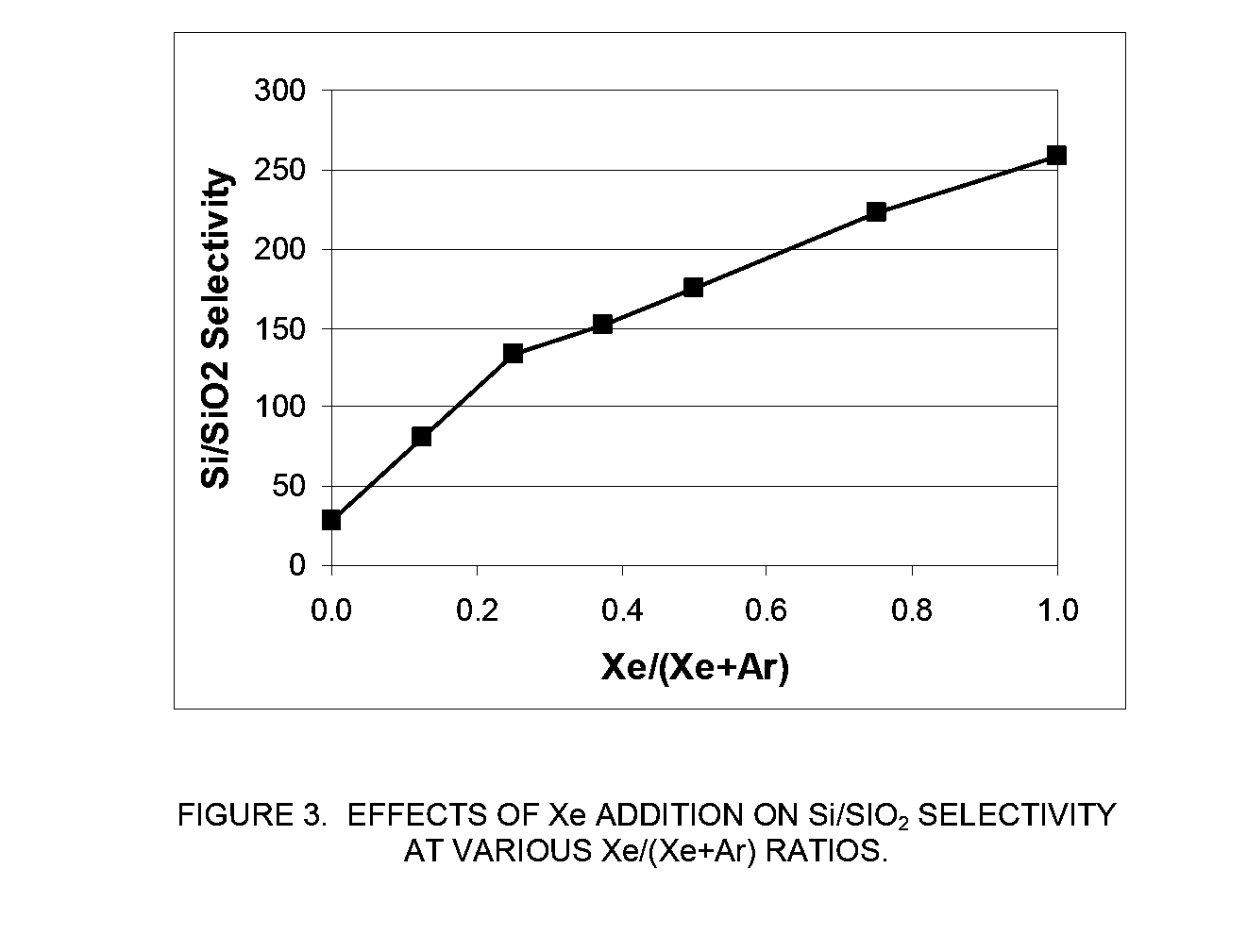
[0071]In this example, an MKS Astron remote plasma generator was mounted on top of a reactor chamber. The distance between the exit of the Astron generator and the sample coupon was about six inches. The remote plasma generator was turned on but the pedestal heater in the reactor chamber was turned off. The chamber was kept at room temperature. The etch rate of both Si and SiO2 substrates using remote plasma was measured.

[0072]The process gas to the remote plasma was NF3 and it was mixed with a second gas stream in various amounts. The second gas stream was comprised of either Xe, argon (Ar), or a combination thereof. The total gas flowrate to the reactor chamber was fixed at 400 sccm and the NF3 flowrate was fixed at 80 sccm. While keeping the total flowrate of the second gas stream at 320 sccm, the ratio of the flowrate of Xe to the total flowrate of the second gas stream (Xe / (Ar+Xe)) was varied between 0 (only Ar as the additional process gas) and 1...

example 3

Selective Etching of Molybdenum(Mo) to SiO2

[0078]A large 2.5 m length 25 cm diameter cylindrical SS etch chamber was used to determine etch rate of another common sacrificial material in MEMS applications: molybdenum (Mo). The remote plasma was generated using a water-cooled MKS Astron AX7670 6 slpm unit. The plasma source was connected to the chamber by a 10 cm long transport tube with a 4 cm inner diameter. The sample was placed 2 feet from the loading / unloading end of the tube.

[0079]At 2.75 torr, 275 sccm NF3 flow and 600 sccm Xe or Ar flow, etch rate of Mo=1.1 microns / min. Etch rate of SiO2 was 82 nm / min for NF3 / Ar gas mixture and was 26 nm / min for NF3 / Xe mixture. Thus, selectivity of Xe / NF3 mixture was at least 3 times that of Ar / NF3 mixture. Note that Mo etch rate is limited by the surface oxide. With a surface preparation treatment to break its native oxide, the etch rate of Mo can be enhanced to >2.7 micron / min.


PUM

PropertyMeasurementUnit
pressureaaaaaaaaaa
temperatureaaaaaaaaaa
Pressuresaaaaaaaaaa

Abstract

This invention relates to a process for selective removal of materials, such as: silicon, molybdenum, tungsten, titanium, zirconium, hafnium, vanadium, tantalum, niobium, boron, phosphorus, germanium, arsenic, and mixtures thereof, from silicon dioxide, silicon nitride, nickel, aluminum, TiNi alloy, photoresist, phosphosilicate glass, boron phosphosilicate glass, polyimides, gold, copper, platinum, chromium, aluminum oxide, silicon carbide and mixtures thereof. The process is related to the important applications in the cleaning or etching process for semiconductor deposition chambers and semiconductor tools, devices in a micro electro mechanical system (MEMS), and ion implantation systems. Methods of forming XeF2 by reacting Xe with a fluorine containing chemical are also provided, where the fluorine containing chemical is selected from the group consisting of F2, NF3, C2F6, CF4, C3F8, SF6, a plasma containing F atoms generated from an upstream plasma generator and mixtures thereof.

Description

CROSS-REFERENCE TO RELATED APPLICATIONS[0001]This application is a continuation-in-part of U.S. patent application Ser. No. 11 / 285,056, filed Nov. 22, 2005, entitled “SELECTIVE ETCHING OF TITANIUM NITRIDE WITH XENON DIFLUORIDE”.BACKGROUND OF THE INVENTION[0002]In the electronics industry various deposition techniques have been developed wherein selected materials are deposited on a target substrate to produce electronic components such as semiconductors. One type of deposition process is chemical vapor deposition (CVD), wherein gaseous reactants are introduced into a heated processing chamber resulting in films being deposited on the desired substrate. One subtype of CVD is referred to a plasma enhanced CVD (PECVD) wherein a plasma is established in the CVD processing chamber.[0003]Generally, all methods of deposition result in the accumulation of films and particulate materials on surfaces other than the target substrate, that is, the deposition materials also collect on the walls,...

Claims


Application Information

Patent Timeline
Patent Type & Authority Patents(United States)
IPC IPC(8): H01L21/302H01L21/461
CPCB08B7/0035C23C16/4405C23F4/00H01L21/32135H01L21/32136H01L21/67028
Inventor WU, DINGJUNKARWACKI, JR., EUGENE JOSEPHMALLIKARJUNAN, ANUPAMAJOHNSON, ANDREW DAVID
Owner VERSUM MATERIALS US LLC
Why Eureka
Try Eureka