
ULTRA-THIN Hf-DOPED-SILICON OXYNITRIDE FILM FOR HIGH PERFORMANCE CMOS APPLICATIONS AND METHOD OF MANUFACTURE

a technology of oxynitride and silicon dioxide, which is applied in the field of semiconductor field effect transistor (mosfet) structures of complementary metal oxide semiconductors, can solve the problems of channel mobile charge scattering, gate structure, conventional method of manufacture, and traditional oxynitride as a gate dielectric material is reaching its technological limits, and achieves the effect of further tinv scaling and device performance enhancemen

Active Publication Date: 2006-10-26
GLOBALFOUNDRIES US INC
View PDF15 Cites 74 Cited by
  • Summary
  • Abstract
  • Description
  • Claims
  • Application Information

AI Technical Summary

Benefits of technology

[0014] The present invention provides a CMOS gate structure that uniformly incorporates a low dose of transitional metal atoms such as Hf, Ti, Zr, or La of below about 7e14 atoms / cm2 or less than a corresponding dose of a continuous metallic film into otherwise thin and uniform layer of oxynitride gate dielectric (9-20 Å in physical thickness) and allows for high mobility of channel carriers (electrons or holes), low density of trapped and fixed charges while providing scaling of Tinv to about or below 16 Å for a conventional polysilicon gate electrode and to about or below 14 Å for a metallic-based gate electrode.

Problems solved by technology

Traditional oxynitride as a gate dielectric material is reaching its technological limits.
Suitable combination of these properties is difficult to achieve with known high-k materials, conventional gate structures, and conventional methods of manufacture.
The very same high polarizability of these bonds results in a scattering of channel mobile charges by remote phonons present in the high-k material.
Accordingly, it is extremely difficult to achieve an ultra-thin high-k-containing gate insulator that does not degrade the carrier mobility in the transistor channel.
While a desirable threshold voltage can be achieved by varying channel doping and selecting a correct work-function of the gate electrode, it can be inadvertently altered by the presence of a large fixed and / or trapped charge at both gate dielectric interfaces and within the dielectric itself.
Further, the density of trapped and / or fixed charge can be inadvertently altered by various processes such as exposure to high-temperature (e.g. a 1000 C junction activation anneal) or during FET operation.
In addition, a high density of fixed or trapped charges in the vicinity of transistor channel can lead to an excessive coulomb scattering of the channel carriers and can reduce the channel mobility and transistor drive current.
As a result, leakage current increases dramatically as the high-K film is thinned.
Further, the highly non-uniform or discontinuous high-k film modulates the electrochemical potential in the transistor channel, and hence, reduces the transistor current.
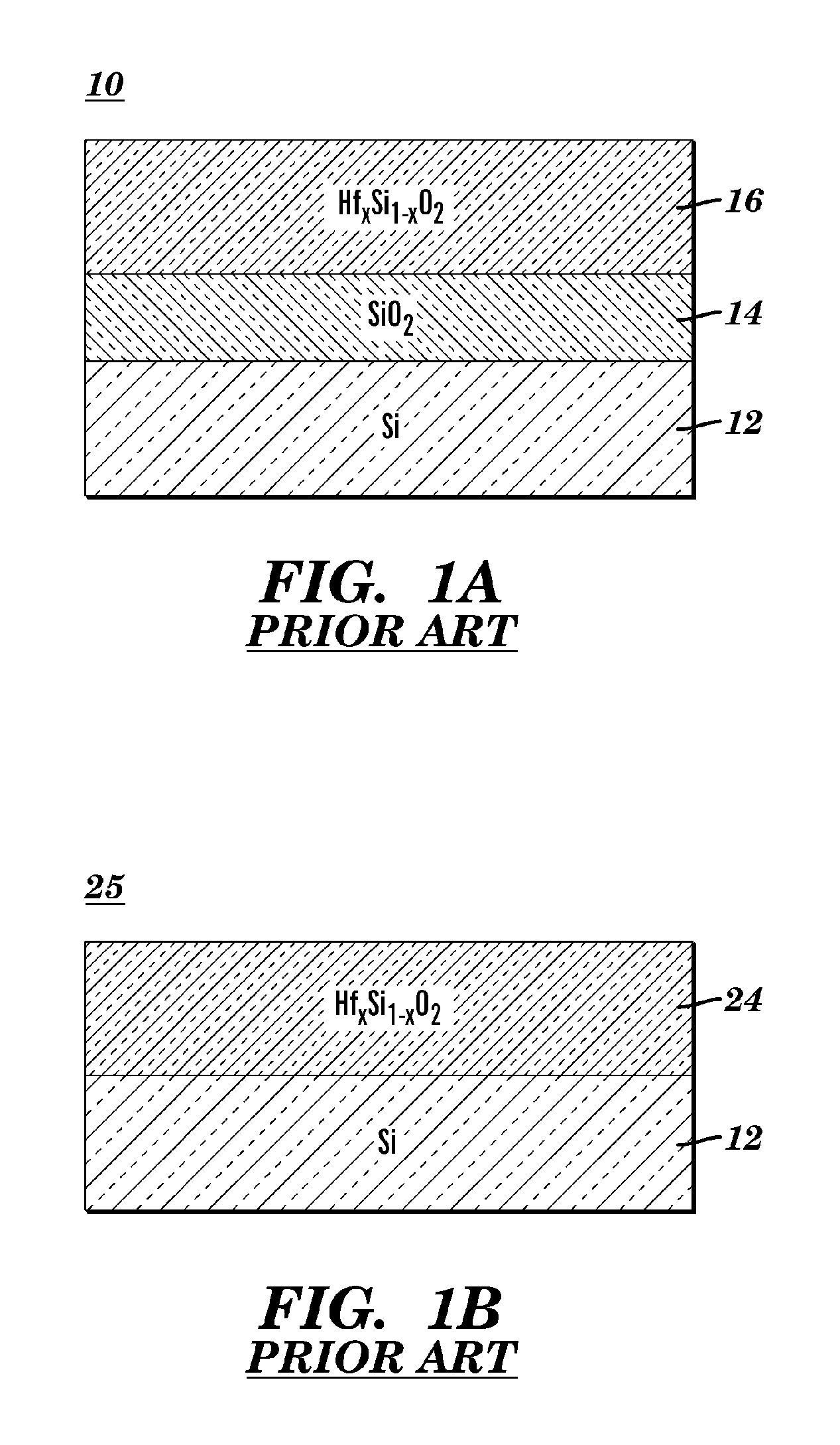
Thus, poor thickness scalability of high-k films results from conventional methods such as the kind illustrated in FIG. 1.
As a result, typical Tinv of the insulating stack 14 / 16 with a continuous 20 Å-thick HfSiO2 film has the following components: dielectric material 14-20 Å, quantum-mechanical 3-5 Å, and depletion of a conventional polysilicon gate electrode 2-5 Å. That is, it is very difficult to scale down a high-k containing insulating layer to meet the requirement of high performance devices (e.g. Tinv<=16.5 A).
The mobility degradation for thinner high-k containing dielectrics is another fundamental challenge for conventional gate dielectric structures and methods of manufacture.
The structure 25 depicted in FIG. 1 (b) further exhibits a high density of interface traps, low mobility and poor thermal stability.
The benefit of this structure is only in the provision of the high-k dielectric due to high dielectric constant without attendant reduction in Tinv to below 16 Å. Furthermore, the '093 patent does not teach any solution to the degraded channel mobility in the case of thin high-k containing dielectrics with Tinv<16 Å. Subsequently, methods taught in the '093 patent are only useful for forming relatively thick high-k containing gate dielectrics that do not suffer much from the mobility degradation effects.
The structure and method disclosed in this patent does not solve the aforementioned high-k scaling problems even though, generally, silicide-based, metal-based, and metallic compound-based (e.g. conductive metal nitrides, borides, carbides, oxides, etc.) gate electrodes result in the reduction or elimination of the depletion portion of Tinv.
As a result, the Tinv of such conventional high-k containing dielectric and FUSI gate electrode is above about 20 Å. Alternatively, the channel mobility is substantially degraded for base SiON layers thinner than about 15 Å and overall Tinv thinner than about 18 Å. While there are numerous instances of prior art teachings where conventional high-k containing films are employed as gate dielectrics in combination with metal gate structures, the resultant transistor gate structures suffer from the same drawbacks as in the '414 Patent and the '874 patent.
Unfortunately, PVD (physical vapor deposition or sputtering) deposition technique employed in the '658 patent Application results in damage to the base oxide film by energetic ions.
In addition, the method is limited to highly reactive titanium atoms which are known to react with silicon oxide at a relatively low temperature of below about 700 C.

Method used


Image

  • ULTRA-THIN Hf-DOPED-SILICON OXYNITRIDE FILM FOR HIGH PERFORMANCE CMOS APPLICATIONS AND METHOD OF MANUFACTURE
  • ULTRA-THIN Hf-DOPED-SILICON OXYNITRIDE FILM FOR HIGH PERFORMANCE CMOS APPLICATIONS AND METHOD OF MANUFACTURE
  • ULTRA-THIN Hf-DOPED-SILICON OXYNITRIDE FILM FOR HIGH PERFORMANCE CMOS APPLICATIONS AND METHOD OF MANUFACTURE

Examples


first embodiment

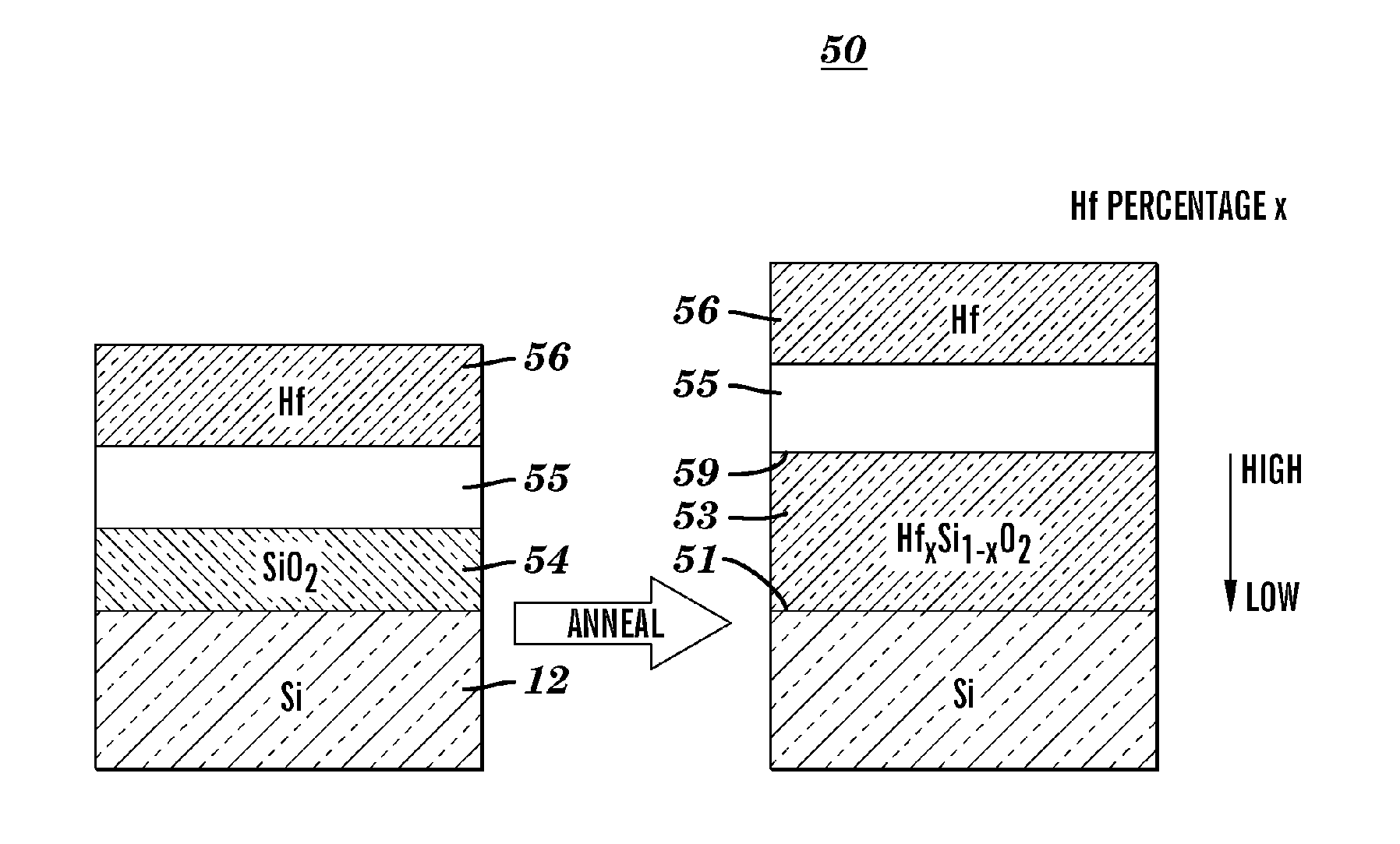
[0046] In a first embodiment, layer 55 is sacrificial and is selected from the following two groups: inert semiconductors and inert metals. Chemical inertness is specified with respect to the layer 54. For instance, germanium (Ge), a preferred representative of the inert semiconductor group, is a relatively stable material with respect to layer 54 and can be very selectively removed in a solution of hydrogen peroxide. A diffusion-controlling Ge layer can be deposited in commercially available CVD reactors using a GeH4 gaseous precursor. Layer 55 is made thick enough (preferably thicker than approximately 100 Å) to circumvent Ge film islanding in the ultra thin regime due to uneven germanium nucleation on the surface of layer 54.

[0047] The preferred inert metals comprise refractory metals and their metallic compounds such as nitrides. These metallic compounds can be selectively removed using a solution of sulfuric acid. Most preferably, the inert metal comprises tungsten (W), molybde...

second embodiment

[0048] In a second embodiment, layer 55 is selected to yield a gate electrode having a suitable work function. Layer 55 can comprise various elemental metals and metallic compounds (e.g. silicides, nitrides, borides, and carbides) which are chemically inert to both layer 54 and transitional metal atoms such as Hf, Ti, La, and Zr. In this case, the material of layer 55 is selected similar to that of a metal gate electrode, that is, its Fermi level is aligned with either conduction or valence band of silicon for conventional NFETs and PFETs, respectively. For example, tungsten nitride with high nitrogen content can be employed as a PFET-compatible gate electrode. Accordingly, layer 55 can comprise WN in the case of PFET devices. In another example, tantalum nitride (TaN) can be employed as a NFET-compatible gate electrode. Accordingly, layer 55 can comprise TaN in the case of NFET devices. While there are many alternative materials for both NFET-compatible and PFET-compatible gate ele...

third embodiment

[0049] In a third embodiment, layer 55 is used to form a gate electrode after reaction with layer 56. Layer 55 is selected to yield a correct work function of the resultant gate electrode. For example, layer 55 can comprise silicon such as amorphous or polycrystalline silicon. Silicon-based layer 55 can be deposited in a low pressure CVD (LPCVD) reactor using silane SiH4 as a silicon precursor. In a typical LPCVD reactor, layer 55 can be made as thin as approximately 50 Å without any loss of continuity. Silicon-based layer 55 can be converted into a silicide-based gate electrode yielding a Fermi level close to the middle point of silicon bandgap. The mid-gap gate electrode is particularly useful for transistors having fully depleted bodies known as fully-depleted transistors.

[0050] Returning to FIG. 5, a source of transitional metal atoms 56 is then formed on top of layer 55. Layer 56 preferably comprises an elemental metal such as Hf, Ti, La, Zr, or an alloy thereof. The metallic l...


PUM


Abstract

A semiconductor structure and method of forming the same, comprising forming a uniform buffer layer of diffusion-controlling stable material on top of a base gate dielectric layer, and then forming a uniform layer which contains a source of transitional metal atoms, and then annealing the structure to diffuse the transitional metal atoms from their source through the diffusion-controlling material and into the base gate dielectric layer.

Description

FIELD OF THE INVENTION [0001] The present invention generally relates to semiconductor devices, and more particularly to complementary metal oxide semiconductor field effect transistor (MOSFET) structures that include a gate stack having an ultra-thin, high-k gate dielectric layer that increases performance of CMOS devices. The present invention also relates to a method of fabricating such MOSFET gate structures having an ultra-thin, high-k gate dielectric layer. BACKGROUND OF THE INVENTION [0002] For a high performance CMOS device, the inversion capacitance-based oxide-equivalent thickness of the gate dielectrics (Tinv) needs to be scaled down below 16 Å for future technologies. Traditional oxynitride as a gate dielectric material is reaching its technological limits. [0003] In future technology generations, it is highly desirable to replace a silicon dioxide or silicon oxynitride dielectric with a gate material that has a higher dielectric constant. These materials are known as “h...

Claims


Application Information

Patent Timeline
IPC IPC(8): H01L29/78H01L21/336
CPCH01L21/28097H01L21/28185H01L21/28229H01L29/517H01L29/4966H01L29/4975H01L21/823857
Inventor ZHU, WENJUANCHUDZIK, MICHAEL P.GLUSCHENKOV, OLEGPARK, DAE-GYUSEKIGUCHI, AKIHISA
Owner GLOBALFOUNDRIES US INC
Learn More