Organic electronic devices incorporating semiconducting polymer brushes

a semi-conducting polymer and electronic device technology, applied in the field of organic electronic devices, can solve the problems of significant loss mechanism in these devices, lack of short and direct transportation paths, and inability to achieve short and direct transportation paths, and achieve the effect of more efficient conversion of photons

Inactive Publication Date: 2007-07-26
CAMBRIDGE UNIV TECH SERVICES LTD
View PDF7 Cites 20 Cited by
  • Summary
  • Abstract
  • Description
  • Claims
  • Application Information

AI Technical Summary

Benefits of technology

[0075] Co-polymerization can be used to grow long polymer brushes consisting of different polymers. A layer of semiconducting material can be percolated through the layer of brushes to obtain a similar structure to that shown in FIG. 3, apart from having co-polymer brushes which conduct one species of charge. In photovoltaic devices, if the different polymers within the brushes have a range of absorption spectra over the solar spectrum, then the final device can be more efficient at converting photons to charges over the solar spectrum. In electroluminescent devices, the colour of the emitted light can be tailored by having different lengths of each block, which emit at different parts of the spectrum. If the electric field dependence of the mobility is vastly different b

Problems solved by technology

However, a significant loss mechanism in these devices is due to charge trapping, caused by a lack of direct transportation paths to each electrode within each component of the blend.
However, significant loss mechanisms in these devices are due to leakage current, caused by percolation paths from cathode to anode within each component of the blend, an imbalance of the charge transportation of holes and electrons to

Method used


Image

  • Organic electronic devices incorporating semiconducting polymer brushes
  • Organic electronic devices incorporating semiconducting polymer brushes
  • Organic electronic devices incorporating semiconducting polymer brushes

Examples


example 2

Silane initiator synthesis—synthesis of 2-bromo-2-methyl-propionic acid 3-trichlorosilanyl-propyl ester

[0097] 2-bromoisobutyryl bromide (1.85 ml, 15 mmol), was added dropwise to a stirred solution of allyl alcohol (1.02 mL, 15 mmol) and triethylamine (2.51 ml, 18 mmol), in DCM (10 ml) at 0° C., under a nitrogen atmosphere. The solution was stirred for 1 hour at 0° C., the temperature was raised to room temperature and the reaction mixture was then stirred for another 3 hours, all under a nitrogen atmosphere. The precipitate was then removed by filtration, the organic layer was washed with saturated NH4Cl, followed by a wash with water. The organic layer was then dried with anhydrous MgSO4 and the solvent evaporated on a rotary evaporator. The product was then purified by column chromatography (silica column) using 9:1 hexane:ethyl acetate as the eluant. The solvent was then evaporated to yield the clear, liquid product prop-2-enyl-2-bromo-2-methyl propionate (1.72 g, 55% yield).

[0...

example 3

Substrate Preparation: Preparation of ITO-Coated Substrate Having a SAM and ITO-Coated Substrate with a PEDOT / PSS Layer Having a SAM

(a) ITO

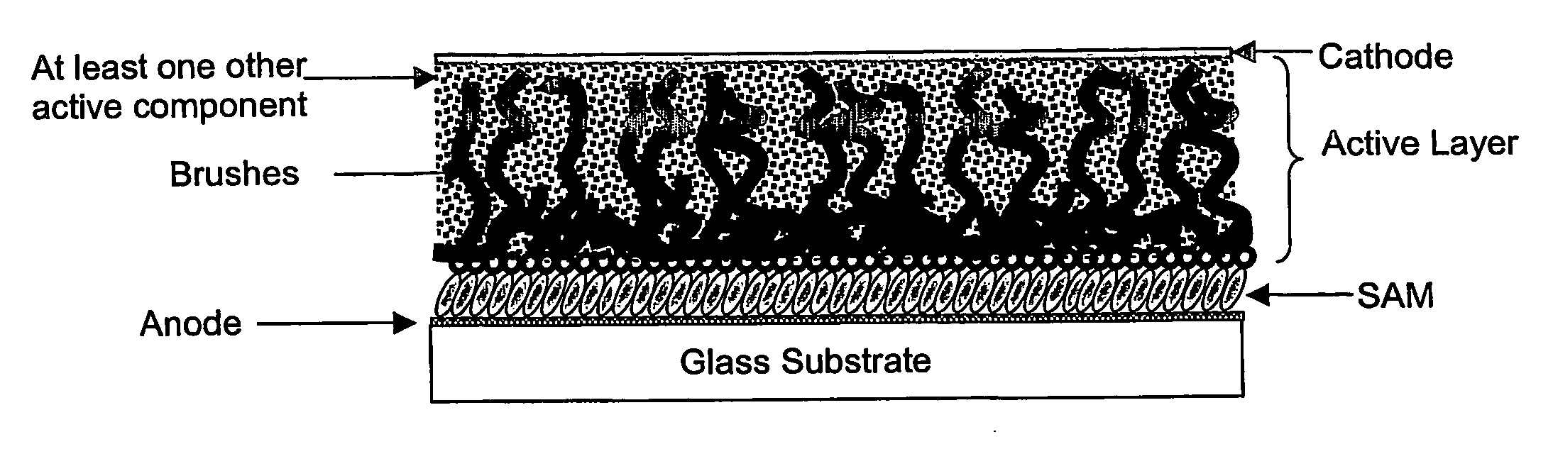
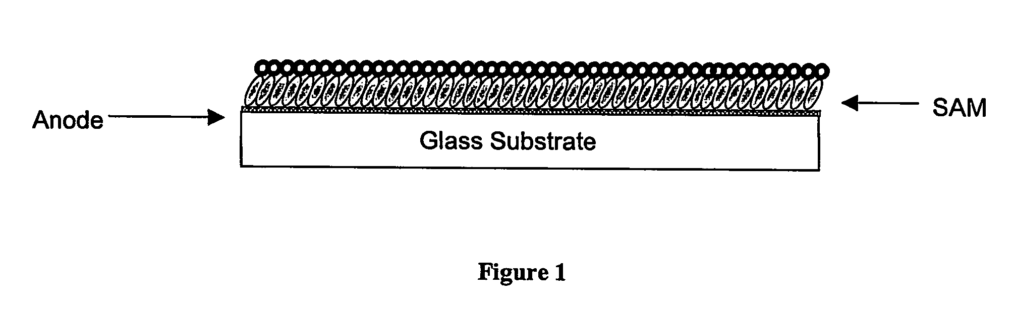
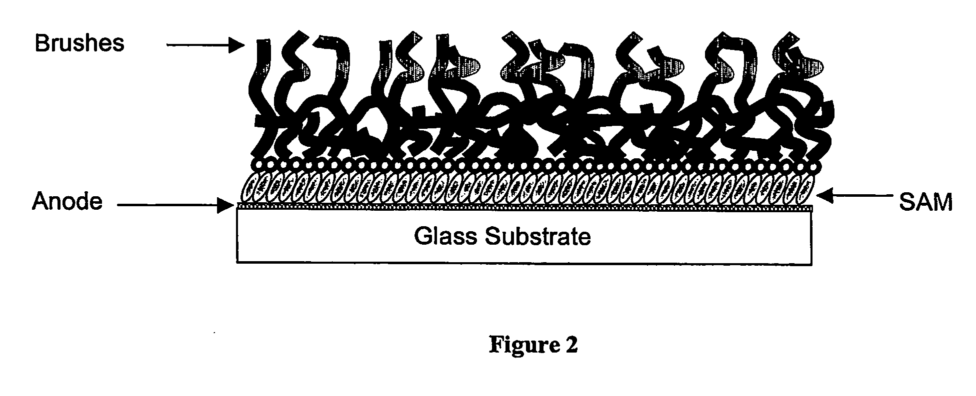
[0099] First, glass pre-coated with ITO (purchased from Donnelly, Inc.) was cleaned by sonicating in acetone (10 mins) and then sonicating in isopropanol (10 mins). The substrate is then made hydrophillic by treating with a 5:1:1 water:ammonia:hydrogen peroxide mixture for 1 hour at 70° C. [alternatively, the substrates could be made hydrophillic using an oxygen plasma treatment (approximately 30 sec at 100 W)]. At the end of this time, the substrate was cleaned, dried, washed with water, dried with a nitrogen gun and then baked in an oven at 100° C. for 24 hours.

[0100] A self-assembled monolayer (SAM) of the initiator prepared in Example 2 above on the hydrophilic ITO-coated substrate obtained above was then prepared either by reacting with said initiator in supercritical CO2 or by reaction in an solution of said initiator in toluene:

[0101]...

example 4

Polymer brush growth: growth of poly(4-diphenylaminobenzyl acrylate) brushes on pre-prepared substrate

[0107] The monomer 4-diphenylaminobenzyl acrylate prepared in Example 1 above was dissolved in solvent (usually DMF) at room temperature (although heating to say 90° C. is typically necessary to completely dissolve the monomer), to give a solution having a concentration of approximately 1 g / ml. A ligand, usually N,N,N′,N′,N″-pentamethyldiethylenetriamine (PMDTA) was added followed by an inhibitor, usually copper (II) bromide. The air in the solution was then replaced with nitrogen by bubbling nitrogen through the solution. A catalyst, usually copper (I) bromide, was then added to the solution thus obtained.

[0108] Separately, one of the substrates with a SAM prepared in Example 3 above was then taken and placed in a Schlenk tube, and the air in the tube replaced with nitrogen by conducting a number of evacuation / refill cycles. The polymerisation solution prepared above was then tra...


PUM

PropertyMeasurementUnit
Lengthaaaaaaaaaa
Lengthaaaaaaaaaa
Lengthaaaaaaaaaa

Abstract

An organic electronic device comprises at least two electrodes and a semiconducting layer comprising a mixture of at least one hole-transporting semiconducting material and at least one electron-transporting semiconducting material, wherein at least one of said semiconducting materials is in the form of semiconducting polymer brushes which are attached to the surface of at least one of said electrodes and are in contact with at least one of said other semiconducting materials. Also provided is an organic electronic device comprising at least two electrodes and a semiconducting layer comprising at least one hole-transporting or electron-transporting semiconducting material, wherein said at least one semiconducting material is in the form of semiconducting polymer brushes which are attached to the surface of at least one of said electrodes. Processes for the manufacture of said devices are also provided.

Description

FIELD OF THE INVENTION [0001] The present invention relates to organic electronic devices such as photovoltaic devices and organic electroluminescent devices, said devices comprising electrodes and a semiconducting layer comprising a mixture of at least one hole-transporting semiconducting material and at least one electron-transporting semiconducting material, wherein at least one of said semiconducting materials is in the form of semiconducting polymer brushes which are attached to the surface of at least one of said electrodes and are in contact with at least one of said other semiconducting materials. It also relates to organic electronic devices such as field effect transistors, said devices comprising electrodes and a semiconducting layer comprising at least one hole-transporting or electron-transporting semiconducting material, wherein said at least one semiconducting material is in the form of semiconducting polymer brushes which are attached to the surface of at least one o...

Claims


Application Information

Patent Timeline
IPC IPC(8): H01L31/00H01L51/00H01L51/30H01L51/50
CPCB82Y10/00Y02E10/549H01L51/0035H01L51/0036H01L51/0037H01L51/0039H01L51/004H01L51/0043H01L51/0044H01L51/0055H01L51/0059H01L51/0075H01L51/0094H01L51/0545H01L51/426H01L51/5012B82Y30/00Y02P70/50H10K85/113H10K85/115H10K85/111H10K85/141H10K85/1135H10K85/154H10K85/151H10K85/623H10K85/631H10K85/701H10K85/40H10K10/466H10K30/35H10K50/11
Inventor HUCK, WILHELM T.S.WHITING, GREGORY L.FRIEND, RICHARD HENRYSNAITH, HENRY
Owner CAMBRIDGE UNIV TECH SERVICES LTD
Why Eureka
Try Eureka