Oftentimes access to a location directly in the path of the load is not practical so that current monitoring is instead performed in an active device,
transistor, or semiconductor component, and preferably in a device controlling the current flow into the circuit from its power input or source, e.g. a generator, battery, or
regulated power supply.
In the event the product of ID and VDS becomes too large for a sustained time interval, the device will overheat and may be damaged.
Current-limiting therefore is often coupled with over-temperature protection circuitry that shuts an overheating device off before irreparable damage occurs to the device or the
system.
Nonetheless, accurate
current limiting demands accurate measurement of a device's current.
It is not always reasonable to assume that assumption is valid.
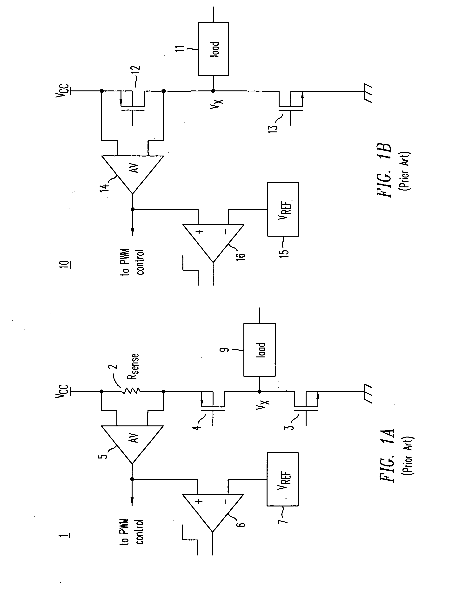
If the resistance Rsense of sense
resistor 2 is too small, the
voltage measured across it will be extremely sensitive to
noise and difficult to measure.
Since the voltage is being measured in the device's main current path, transients, current spikes, and capacitive displacement currents appear instantly as a
signal on the input of
amplifier 5, causing a noisy and jittery output.
Conversely, if the value Rsense is too large, excessive I2·Rsense power dissipation will occur in
resistor 2, degrading efficiency and leading to unwanted die heating.
The accuracy of such a circuit will be very poor, since variations in the offset voltage of
amplifier 5 can vary by several milli-volts from one
wafer lot to another.
To minimize this sensitivity, a 5 mΩ resistor exhibits a more measurable 10 mV drop across resistor 2, but unfortunately represents a 50% increase in power dissipation beyond the MOSFET's losses, meaning the total loss increases from 80 mW without the sense resistor to 100 mW, an overall increase of 25%.
Also, as the magnitude of the offset and the measured value approach one another, i.e. as Vsense→Voffset, the current sense accuracy becomes very poor and can vary by 30% or more, even if a more expensive precision current sense resistor is used.
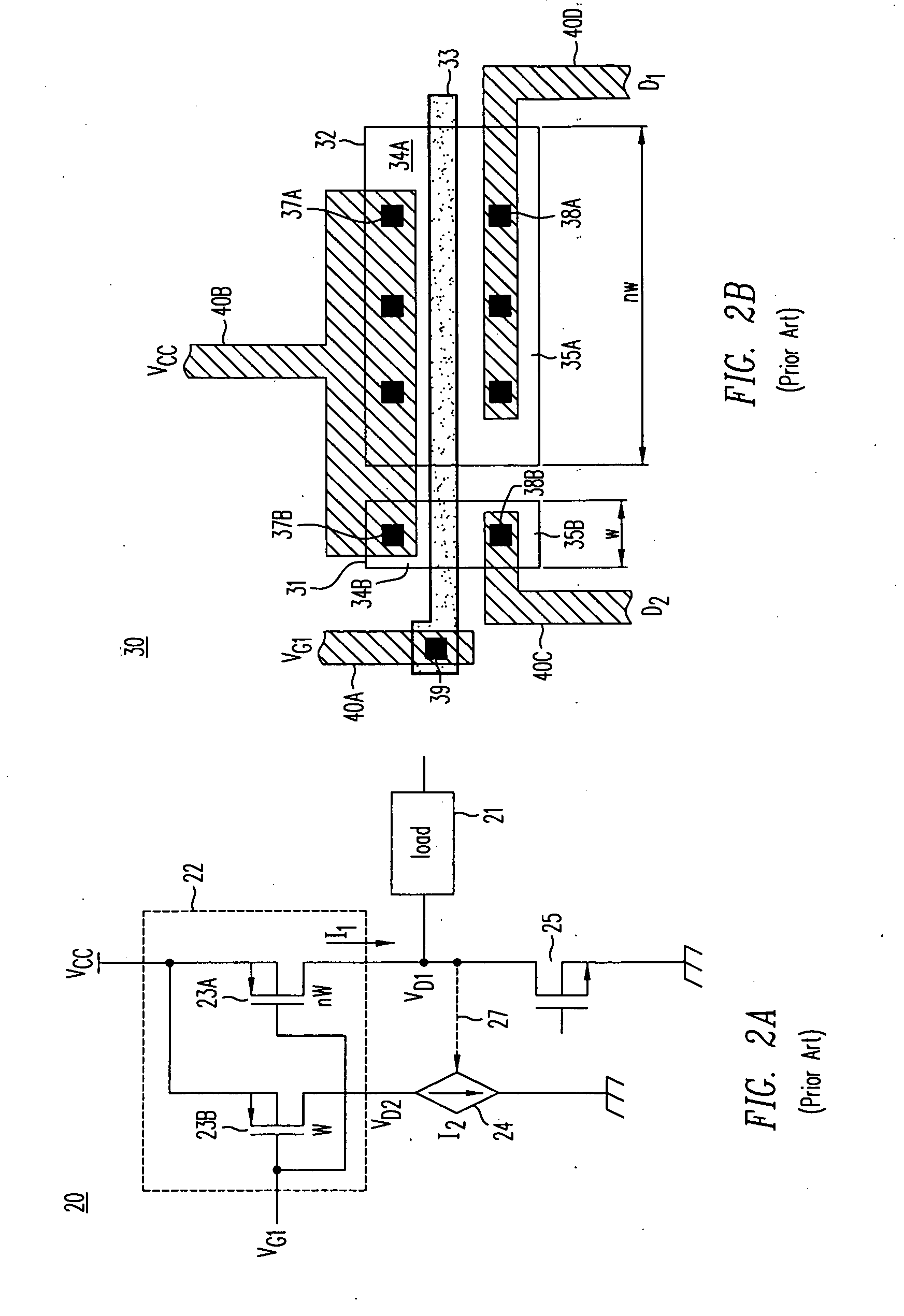
This approach can help to some degree, but it is limited in switching circuits because any increase in the size of MOSFET 4 increases its
capacitance and this causes a corresponding increase in switching losses.
One major problem with VDS sensing is it relies on the resistance of the
power MOSFET to determine the current.
Unfortunately, the resistance of a
power MOSFET is sensitive to a myriad of electrical and process related parameters.
In operation, dynamic and constant variations in VGS, VDS and temperature conditions all affect a MOSFET's resistance and disturb the circuit's ability to accurately detect current.
A change in packaging, vendor,
wafer fab, or heat sinking could cause the VDS sensing and over-current protection circuitry to fail altogether.
In some instances,
system designers have been known to intentionally change the size and on-resistance of a
power MOSFET in an application not realizing they inadvertently disabled operation of the over-current protection.
Since VDS sensing relies on a device behaving as a semi-constant resistance, it cannot be used to detect current in IGBT's, thyristors, diodes or any device that includes minority carrier transport or
conductivity modulation, since such devices do not manifest a linear voltage-current relationship.
VDS sensing also cannot monitor
diode current in a power MOSFET and does not detect avalanche current.
Another complication of using VDS sensing is that
operational amplifier 14 is subjected to the same voltages, voltage transients and spikes as power MOSFET 12 and must be able to survive these voltages without damage.
Even more complex, the operation of the VDS over-current detection circuitry must be disabled whenever MOSFET 12 is turned off or undergoing a switching transient, e.g. when the device is conducting current while VDS is momentarily large.
Device dimensions in integrated circuits and most components are too small to generate substantial magnetic fields.
Detection sensitivity is equally problematic, since other causes may disturb the magnetic sensor and give false readings.
Finally, most magnetic detection systems have a fairly low bandwidth and are incapable or reacting to the
microsecond changes common in electrical systems and voltage regulators.
Currents below one microampere are more noise sensitive and ill advised.
Any slight deviation in VDS on the current sense device, i.e. where VD2≠VD1, results in a dramatic change in the current ratio and a
significant error in measuring the current.
Despite its numerous benefits, however, the split-
drain current-mirror current sensing technique suffers from a number of significant deficiencies.
One major
disadvantage of this circuit is that the drain of the main power MOSFET, often the noisiest and highest voltage node in a
system, must be monitored in order to control the current biasing the current sense MOSFET.
Moreover, any voltage error in the
operational amplifier due to input voltage offset is manifested as a current mismatch and an error in the circuit's ability to accurately measure current.
Another limitation of sensing current with a split-drain MOSFET current-mirror sensing technique is that it is unable to measure avalanche current or forward biased
diode current.
As a result, it cannot detect certain fault conditions that the sense resistor method of FIG. 1A can detect.
The greatest limitation of the split drain MOSFET
current sensor, however, is its technological specificity—it can only be fabricated in planar power devices, and planar MOSFETs suffer from many limitations.
Despite their versatility, such devices suffer from numerous restrictions inherent in their construction.
These limitations
restrict the use of planar power MOSFETs in a variety of areas, including voltage scaling, reliability and circuit topology.
Voltage Scaling Limitations in Planar MOSFETs: Lateral MOSFETs produced using a planar
CMOS fabrication process have a limited voltage
scalability.
So while low-voltage lateral MOSFETs can be made with low on-resistance, high-voltage lateral MOSFETs have a limited
power handling capability.
Metal resistance and
high voltage reliability considerations further degrade the capability of lateral MOSFETs.
Accordingly, while a lateral MOSFET can easily monitor current using a split-
drain current mirror method, it is not very useful as a main power MOSFET.
In some cases, it can short the gate entirely and kill the device.
Such hot carrier-induced damage and especially
hot electron injection or HEI-induced damage is virtually unavoidable in lateral MOSFETs formed at the
silicon surface.
The problem becomes even worse at high voltages, where the
conductivity of lightly-doped drain extensions can become modulated by
impact ionization and pre-avalanche conditions.
This
snapback problem in a device conducting current is known as a limitation in its “safe-operating-area”.
Snapback in the off-state when the device is driven into avalanche is referred to as a limitation in the ruggedness of the device.
Regardless of whether the failure of the device is instantaneous in avalanche or in its safe-operating-area, or a gradual hot carrier-induced degradation, a lateral MOSFET's reliability and
survivability can only be improved by limiting its
current density, increasing its
breakdown voltage, or limiting its maximum
operating voltage.
Unfortunately, running a device at a lower
current density means the device must be oversized for its current rating, i.e. the device will be too big and too expensive a solution to be competitive in the marketplace.
Increasing a lateral MOSFET's
breakdown voltage adds series resistance to the device, again making the device too big and limiting it to non-
power control circuit applications.
And since many power applications operate at voltage above 5V, e.g. at 12V, 18V, 30V, 60V and even several hundred volts, limiting the device's maximum applied voltage is not an option.
Conversely, sensing current in high-side N-channel MOSFETs or in floating
synchronous rectifier N-channel MOSFETs with integrated source-body shorts requires a more complex fabrication process to form
electrical isolation.
Since, without isolation, only P-channel MOSFETs may be used on the high-side, the
power level achievable by
integrated devices is limited to lower voltages and lower currents.
Current Sensing in Vertical DMOS: Unfortunately all vertical DMOS cells, whether planar, trench-gated or super-junction, share a
common drain and substrate.
It is extremely difficult to separately detect current in the two devices in this configuration.
No resistor can be inserted into the grounded source of
low resistance DMOS 251A without degrading its performance and increasing conduction losses.
As a result, source voltage VS2 is no longer the same potential as grounded VS1, and a measurement error results.
With differing gate-to-source and drain-to-source voltages, the mismatch in current can be severe.
Attempts to force VS1 and VS2 to the same level are problematic, not only complicating the bias circuitry, but making the
signal across sense resistor 273 too small for
amplifier 274 to detect.
For the above reasons, the split-source vertical DMOS does not facilitate a useful
current mirror.
Sensitive to both VGS and VDS mismatches, the split source sense MOSFET is vastly inferior to and incompatible with the more normal split drain circuitry described previously.
Unfortunately, the split drain device cannot be integrated into any vertical DMOS
transistor, whether planar, trench or super-junction.
These limitations, practically speaking, relegate all of today's vertical DMOS to the current sense resistor and VDS sensing methods for monitoring current.
The problem is further exacerbated in high power devices.
Current Sensing in High Power Devices: Unfortunately, vertical devices capable of delivering
higher power to a load, especially those in high-voltage applications, comprise device structures and use technology not amenable to the aforementioned integrated
current mirror and VDS sense current
monitoring methods.
Such high power devices, including thyristors, gate turn-off thyristors or GTO's, insulated-gate bipolar transistors or IGBT's, utilize some mix of minority carrier and majority
carrier current flow, making it virtually impossible to integrate the current sensing within the high power device.
Specifically, minority carrier conduction easily shorts-out or bypasses any integrated sensing method.
But because the currents are high, the
voltage drop across the resistor can cause increased power dissipation.
As shown, the series sense resistor is most versatile but increases power losses by inserting a series resistance in the
high current path.
The resistor's
power loss can be reduced by lowering the resistor's value, but this adversely results in a smaller signal and greater
noise sensitivity.
This tradeoff is a fundamental limitation of the otherwise versatile sense resistor method.
Integrating the sense resistor into the device being measured is ill advised, limiting its accuracy by subjecting it to heating,
package stress, and electrical noise.
Referring again to Table 1, VDS sensing is much less accurate than using a precision sense resistor because it is sensitive to temperature, bias conditions, and noise and it is only applicable to MOSFETs operating in their linear operating region.
VDS sensing does not work for devices with
diode conduction, in avalanche, employing minority carrier conduction, or otherwise exhibiting non-linear current-voltage characteristics.
The split-
drain current mirror is good for monitoring the current in integrated lateral devices, but such devices are useful only for
low voltage operation, primarily below 20V.
It cannot be integrated into vertical devices.
It is also not useful in diodes or devices exhibiting diode conduction, devices with minority carrier conduction, or operating in avalanche.
The split-source
current mirror or sense FET suffers numerous disadvantages compared to the split-drain current mirror, and it requires complex biasing to minimize the influence of source voltage biasing from causing both VDS and VGS mismatch error in its current measurement.
Aside from its severe bias sensitivity, it also is subject to temperature variation, and noise, and incompatible with devices operating in
avalanche breakdown, with diode conduction, or exhibiting minority carrier conduction.
In conclusion, as shown in Table 1, no current sensing method available today is able to accurately measure current for the full range of available discrete and integrated power devices.

