Thin film-laminated polyimide film and flexible printed wiring board

a technology of flexible printed wiring board and thin film, which is applied in the direction of printed circuit non-printed electric components association, transportation and packaging, synthetic resin layered products, etc., can solve the problems of inferior shape retainability and stiffness of conventionally known substrate films made of polyimide films or polyimide benzoxazole films, and easy warpage and distortion. , to achieve the effect of superior flat plane retention, superior adhesion of metal thin film layers, and superior plan

Inactive Publication Date: 2009-03-05
TOYO TOYOBO CO LTD
View PDF17 Cites 13 Cited by
  • Summary
  • Abstract
  • Description
  • Claims
  • Application Information

AI Technical Summary

Benefits of technology

[0114]The thus-obtained metallized polyimide film of the present invention is subjected to the steps for application of a photoresist to a conductive metal thin film layer and/or a metal thick film layer side, drying, exposure, development, etching and photoresist release by a conventional method to form a wiring circuit pattern, and further to application of solder resist, curing and electroless tin plating as necessary, whereby a flexible printed circuit board, a multi-layer printed circuit board comprising multiple layers thereof, or a printed circuit board containing a semiconductor chip directly mounted thereon is obtained.
[0115]A coated film of an inorganic material such as a simple metal, metal oxide and the like may be formed on the surface of a metal thin film layer and/or a metal thick film layer (copper layer) used in the present invention. In addition, the surface of a metal thin film layer and/or a metal thick film layer may be subjected to a treatment with a coupling agent (aminosilane, epoxysilane and the like), a sandblast treatment, a holing treatment, a corona treatment, a plasma treatment, an etching treatment and the like.
[0116]As mentioned in the foregoing, a metallized polyimide film using a polyimide film having particular property as a substrate is superior in the planarity and when processed, for example, into a printed circuit board and the like, it is free of warpage and distortion, showing superior flat plane retention as well as superior adhesion of a metal thin film layer. Since uniform laminate processing is possible even when multiple layers are formed, the film shows small warpage and deformation and is useful as a substrate for mounting display driver, high-speed arithmetic device, graphic controller, high capacity memory element and the like requiring particularly high...

Problems solved by technology

Conventionally known substrate films made of a polyimide film or a polyimide benzoxazole film are inferior in the shape retainability and stiffness as compared to substrates made of ceramic.
In addition, they have problem of easy occurrence of warpage and distortion during production of electronic parts due to the property difference within the film.
Particularly, film warpage and distortion easily occurred during lamination of a thin film on a substrate film by dry plating.
However, even if apparent film war...

Method used


Image

  • Thin film-laminated polyimide film and flexible printed wiring board
  • Thin film-laminated polyimide film and flexible printed wiring board

Examples


examples

[0141]The present invention is explained in more detail in the following by referring to the Examples and Comparative Examples below, which are not to be construed as limitative. The evaluation method of the properties in the following Examples are as shown below, wherein the degree of curl after a heat treatment at 300° C. is based on the aforementioned method.

1. Thickness of Polyimide Film

[0142]A micrometer (Millitron (registered trade mark) 1245D manufactured by FEINPRUF) was used for the measurement.

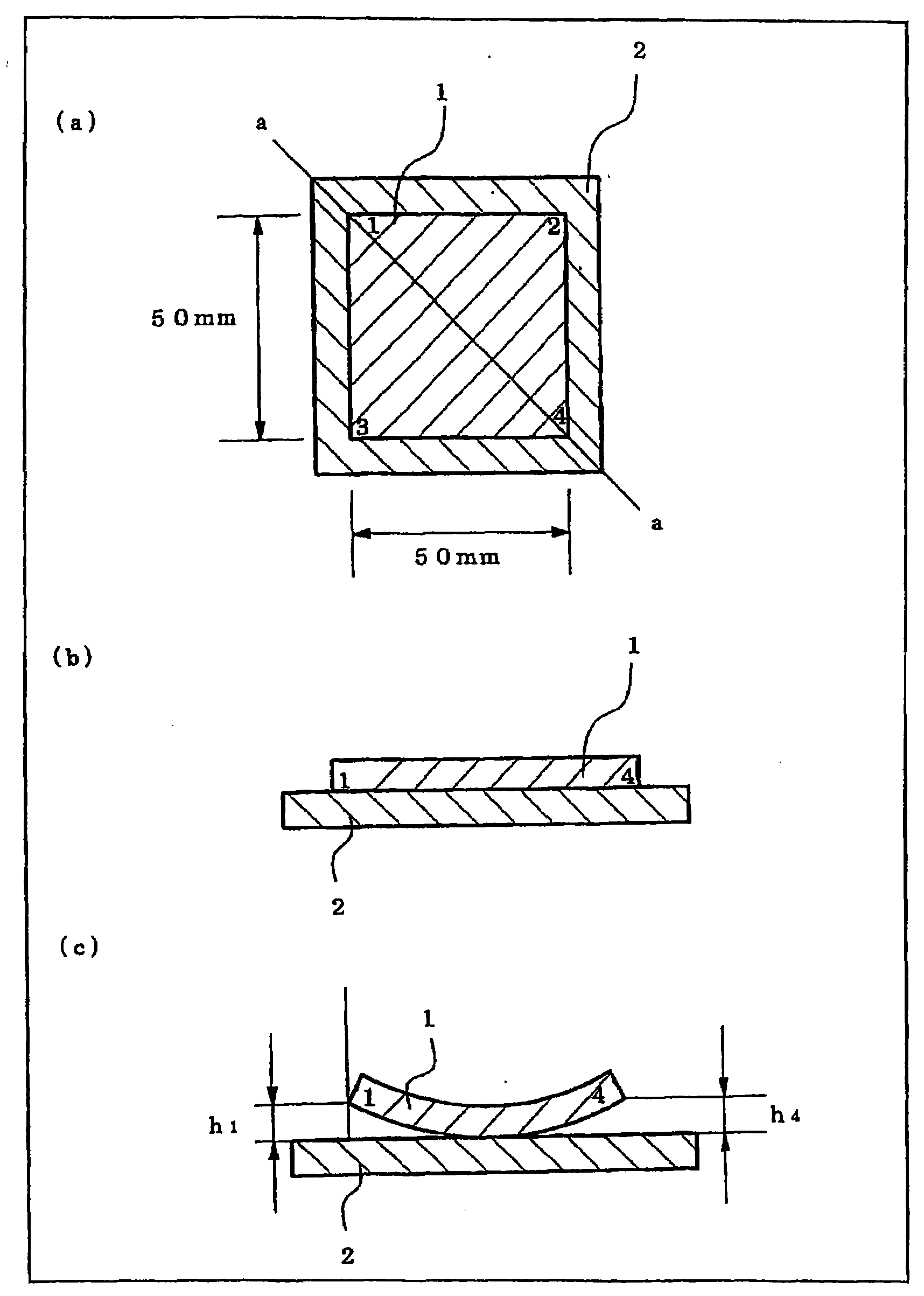
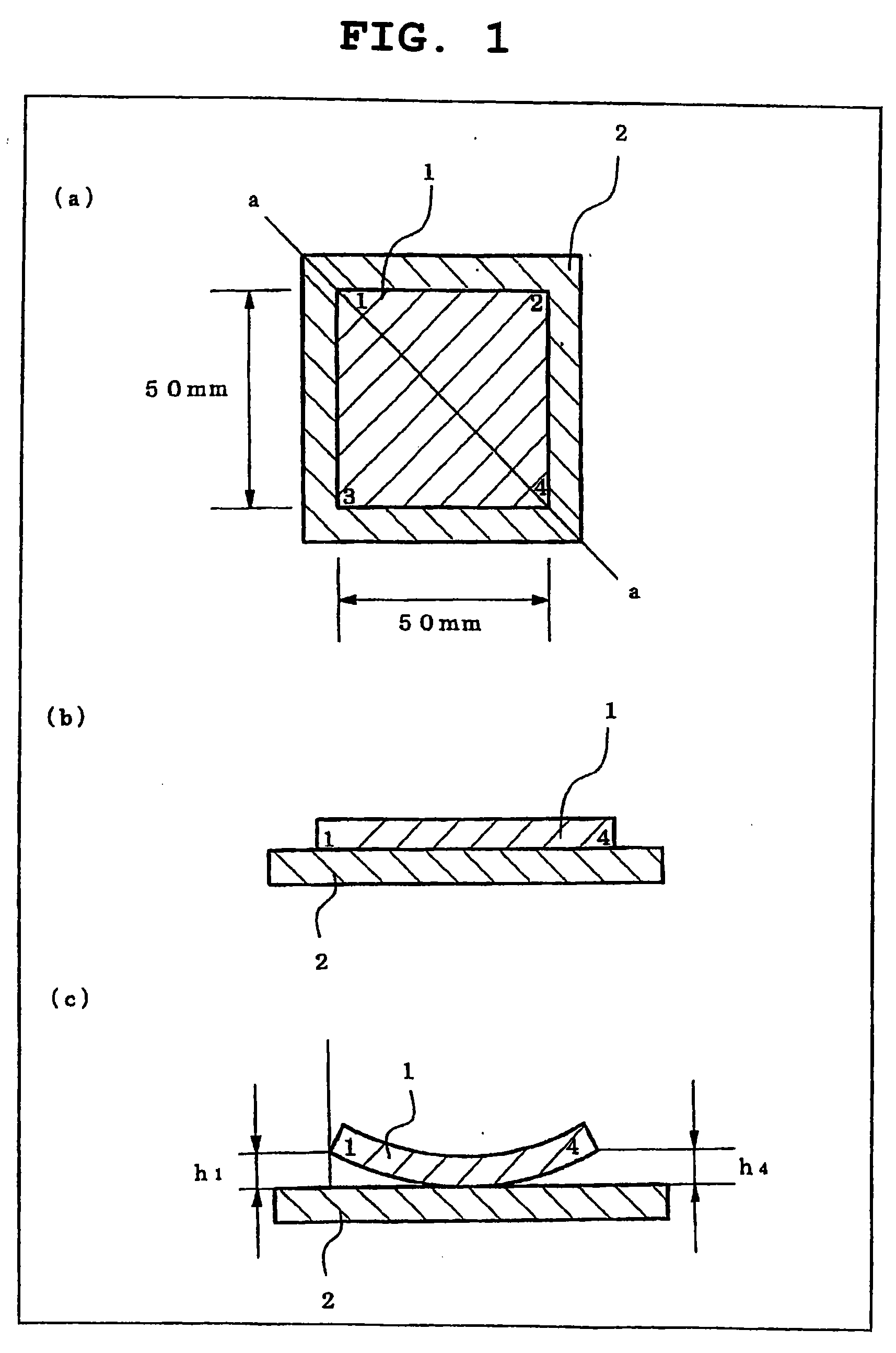
2. Degree of Warpage of Film (Apparent Degree of Warpage)

[0143]As shown in FIG. 1(C), a 50 mm×50 mm film test piece was stood still on a flat plane to form a concave, an average distance from each top point on the test piece to the flat plane (h1, h2, h3, h4: unit mm) was taken as the amount of warpage (mm), and a value shown by the percentage (%) of the amount of warpage relative to the distance (35.36 mm) from each top point on the test piece to the center was obtained.

[0144]Specif...

production examples 1-3

[0157]A container equipped with a nitrogen inlet tube, a thermometer and a stirrer bar was substituted with nitrogen, and P-PDA was placed therein. Then, DMAC was added and, after complete dissolution, BPDA was added, and the mixture was polymerized by stirring at 25° C. for 5 hr at a molar ratio of P-PDA and BPDA as monomers of 1 / 1 in DMAC while adjusting the monomer charge concentration to 15 mass %. As a result, a brown viscous polyamic acid solution was obtained. AA (15 parts by mass) and IQ (3 parts by mass) were added per 100 parts by mass of the obtained polyamic acid solution, and the mixture was applied to the lubricant-free surface of a polyester film (COSMOSHINE (registered trade mark) A4100, manufactured by Toyo Boseki Kabushiki Kaisha) having a thickness of 188 micron and a width of 800 mm, in a coating width of 740 mm (squeegee / belt gap 430 μm). The film was dried during passage through a continuous drying furnace having 4 drying zones. In each zone, 3 rows of slit-lik...

production examples 4-6

[0177]A container equipped with a nitrogen inlet tube, a thermometer and a stirrer bar was substituted with nitrogen, and P-PDA was placed therein. Then, DMAC was added and, after complete dissolution, BPDA was added, and the mixture was polymerized by stirring at 25° C. for 5 hr at a molar ratio of P-PDA and BPDA as monomers of 1 / 1 in DMAC while adjusting the monomer charge concentration to 15 mass %. As a result, a brown viscous polyamic acid solution was obtained. The obtained polyamic acid solution was applied to a stainless belt (gap between squeegee / belt 450 μm), and dried in the same manner as in Production Examples 1-3. By releasing the polyamic acid film that became self-supporting after the drying from the stainless belt, each green film, i.e., Production Example 4, Production Example 5 and Production Example 6 were obtained.

[0178]The obtained green films were subjected to 2-step heating under the conditions of first step: 180° C., 3 min, temperature rise rate 4° C. / sec, s...


PUM

PropertyMeasurementUnit
Temperatureaaaaaaaaaa
Fractionaaaaaaaaaa
Temperatureaaaaaaaaaa

Abstract

The thin film-laminated polyimide film contains a substrate film and a thin film layer formed at least on one surface of the substrate film. The substrate film is made of a polyimide film showing a degree of curl after a heat treatment at 300° C. of not more than 10%. Use of this thin film-laminated polyimide film as a substrate of electronic parts such as solar battery, capacitor and the like exposed to high temperatures prevents easy development of warpage and distortion during production, and can improve quality and yield of electronic parts.

Description

TECHNICAL FIELD[0001]The present invention relates to a thin film-laminated polyimide film used for a flexible printed circuit substrate and the like that play an important role in the down-sizing and lightening of electronic devices and electronic parts. More particularly, the present invention relates to a thin film-laminated polyimide film to be used for a flexible printed circuit substrate subjected to TAB, COF, PGA etc. for semiconductor packaging and the like, which comprises a polyimide film having particular properties as a substrate film, wherein the thin film-laminated polyimide film made conductive shows less warpage and curling.BACKGROUND ART[0002]Conventionally, metallized polyimide films to be used for what is called bonding type flexible printed circuit substrates, in which a polyimide film is bonded with a metal foil such as copper foil, aluminum foil and the like with an adhesive, are known. Such films have the following problems considered to be attributable to the...

Claims


Application Information

Patent Timeline
IPC IPC(8): H05K1/18B32B27/06B32B15/08
CPCH05K1/0346H05K3/181H05K3/388H05K2203/065H05K2201/0317H05K2201/0326H05K2201/0154Y10T428/31721Y10T428/31681B32B27/34
Inventor MAEDA, SATOSHIKAWAHARA, KEIZOTSUTSUMI, MASAYUKIYOSHIDA, TAKEFUMI
Owner TOYO TOYOBO CO LTD
Why Eureka
Try Eureka