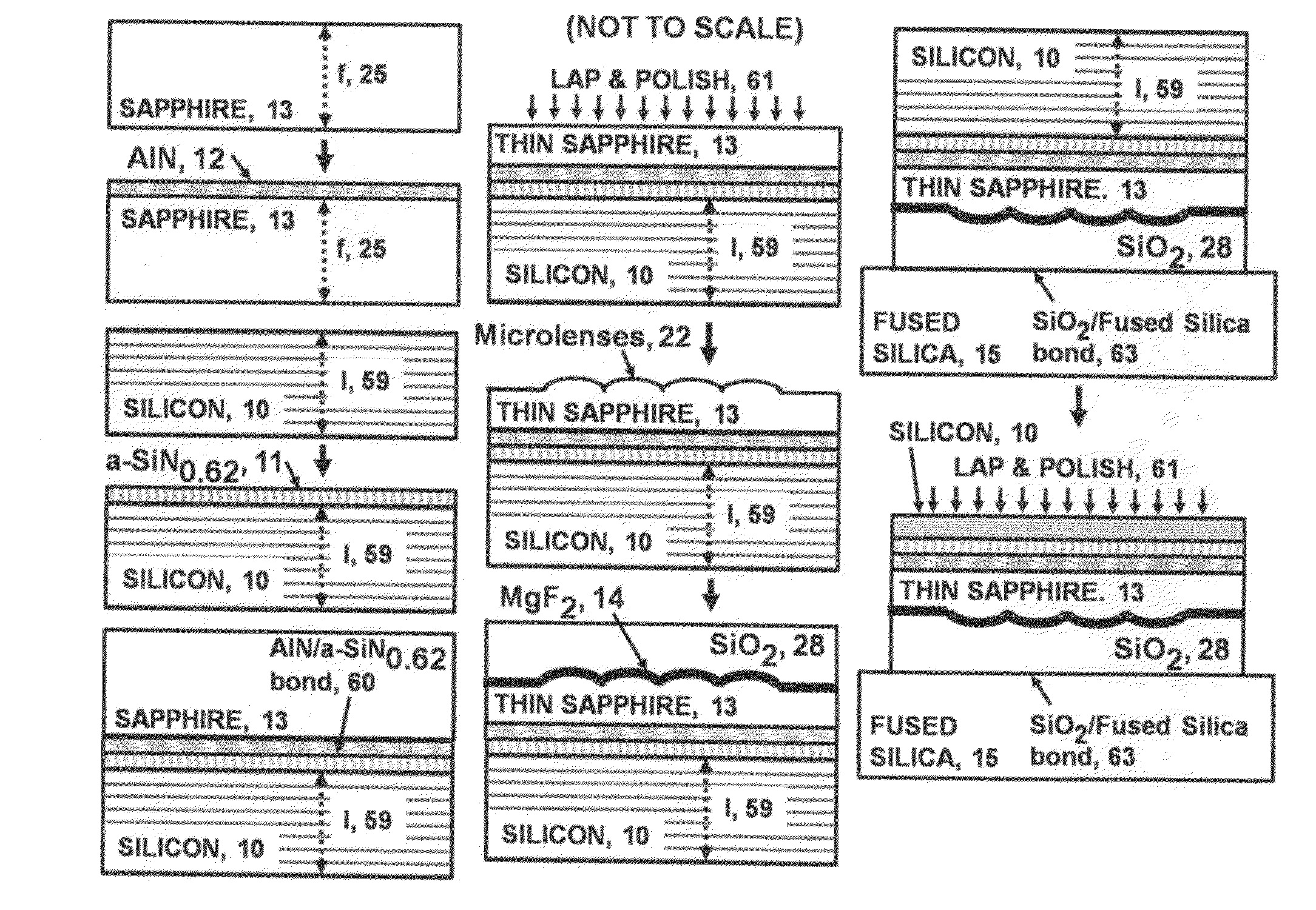
[0020]The advanced silicon-on-
sapphire substrate that is the subject of the present invention solves the problem of
thinning the sapphire to an optimum thickness needed for
light transmission into silicon and the suppression of indirect optical
crosstalk, by bonding the sapphire or λ / 4-MgF2 antireflective layer
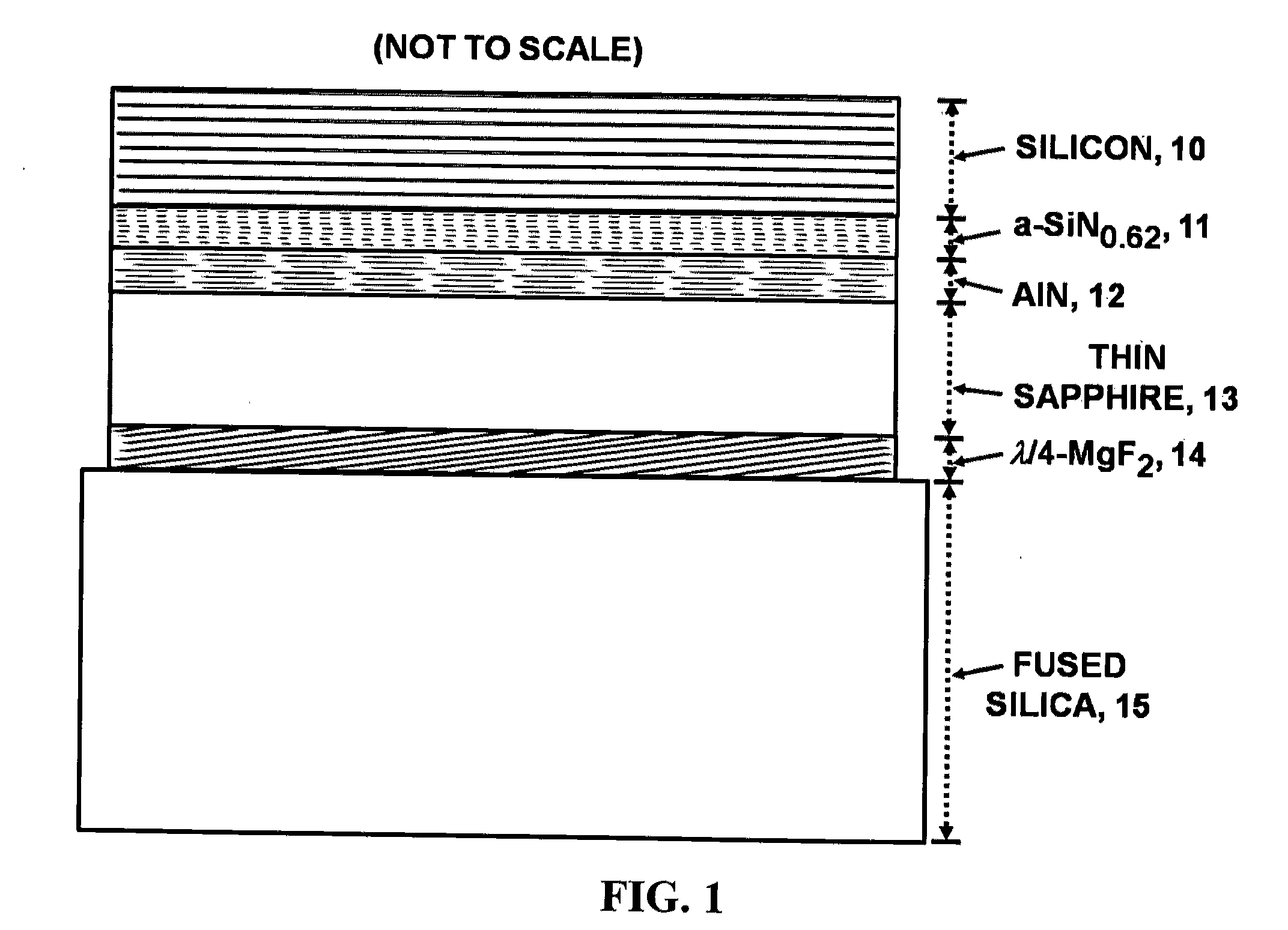
coating the sapphire back-side, to a dissolvable fused silica substrate. The fused silica substrate provides mechanical support for the optimally thinned sapphire, during solid-state device fabrication. After device fabrication the thin silicon-on-sapphire can be recovered by
coating the silicon with a
photoresist layer and immersing the wafer into buffered
hydrogen fluoride (HF)
etching solution that dissolves the fused silica, leaving the silicon-on-sapphire unaffected. To further improve the back-illuminated
optical transmittance into silicon, the substrate incorporates an antireflective
bilayer comprised of
single crystal aluminum
nitride (AlN) and amorphous, non-stoichiometric
silicon nitride (a-SiNX<1.33) referred to as (AlN / a-SiNX<1.33) between sapphire and silicon. By selecting the proper composition for the non-stoichiometric, silicon rich a-SiNX<1.33 layer, thereby also tuning its
refractive index, it becomes possible to provide nearly optimal
refractive index matching in conjunction with the
single crystal AlN, between the
sapphire substrate and the
silicon detector device layer. Selecting the proper thickness for the AlN as well as the proper thickness and
stoichiometry for a-SiNX<1.33 will result in nearly optimal
broadband optical transmittance from sapphire into silicon. An amorphous, one quarter
wavelength magnesium fluoride (λ / 4-MgF2) antireflective layer deposited on the back surface of the thinned
sapphire wafer improves the optical
transmittance from the ambient into the sapphire.
[0022]The thin, very
high transmittance, back-illuminated silicon-(AlN / a-SiNX<1.33)-sapphire substrate with λ / 4-MgF2 back-side antireflective layer bonded to fused silica, readily supports fabrication of silicon mesa detectors with exposed (111) side planes and fixed crystallographic angle φC=54.7° between (100) and (111) silicon planes, by liquid
anisotropic etching using tetramethyl
ammonium hydroxide (TMAH) to define the APD
detector array. The AlN / a-SiNX<1.33 antireflective
bilayer and sapphire act as natural etch stopping
layers to enable fabrication of highly uniform silicon mesa pixels by crystallographic
etching. In addition, monolithic sapphire microlenses can be fabricated beneath each mesa APD detector pixel in the thinned sapphire to focus light under the full height of the detector mesas and also contribute to indirect optical crosstalk suppression by multiple reflections in the sapphire of the APD emitted light. The space between mesa APD detector pixels can be filled by an aluminum (Al) or
copper (Cu)
metal anode grid, forming a common
anode electrical connection at the base of each
silicon detector mesa. The Al
metal common
anode grid also performs the important secondary function of providing optical crosstalk isolation for direct
line of sight light propagation between adjacent APD detectors by blocking light emitted during the avalanche
gain process.
[0023]The design of the thin, very
high transmittance, back-illuminated silicon-(AlN / a-SiNX<1.33)-sapphire-(MgF2)-fused silica substrate allows the complete substrate to be fabricated prior to the fabrication of Si or SiGe APD detectors in the silicon device layer, since none of the material
layers in the substrate including AlN, a-SiNX<1.33, sapphire or MgF2 will be adversely affected by subsequent APD detector device fabrication in the silicon mesas using conventional silicon
processing technology (e.g.
thermal oxidation,
diffusion of
dopant impurities, deposition and metallization steps). The fused silica might be etched slightly with the conventional silicon
processing for devices that might include isotropic liquid
etching with HF, however, this is not problematic since the fused silica will be dissolved in buffered HF after device fabrication, to recover the thin silicon-(AlN / a-SiNX<1.33)-sapphire-(MgF2) substrate. The capability to fully fabricate and characterize the very high
transmittance, back-illuminated silicon-(AlN / a-SiNX<1.33)-sapphire substrates with back-side λ / 4-MgF2 antireflective layer prior to fabricating the silicon detectors is cost effective, first, by allowing wafer substrates to be optimally fabricated, separately and independently from the detector devices, and second, by preventing the consumption of expensive
semiconductor gases to manufacture detectors in unfinished wafer substrates that might not pass quality standards once fully fabricated.
[0024]In summary, an optimized thin, silicon-(AlN / a-SiNX<1.33)-sapphire substrate with back-side λ / 4-MgF2 antireflective layer bonded to dissolvable fused silica, having a properly designed thickness of AlN and MgF2 layers as well as properly designed thickness and composition of a-SiNX<1.33, can achieve nearly 100% back-illuminated optical
transmittance over a broad
wavelength range from 250-1100 nm. The thin, very high transmittance substrate will support the fabrication of high
quantum efficiency and
high resolution, back-illuminated silicon and silicon-
germanium APD detector arrays with effective direct and indirect optical crosstalk isolation between neighboring and distant pixels in the array. The thin, silicon-(AlN / a-SiNX<1.33)-sapphire substrate with back-side λ / 4-MgF2 antireflective layer bonded to fused silica can be fabricated separately and independently from the detector device arrays. Thus, there is no need to potentially waste expensive resources to manufacture detector arrays in unfinished wafer substrates that might not pass quality standards once fully fabricated.

