Ultrathin high-K gate dielectric with favorable interface properties for improved semiconductor device performance

a dielectric and interface technology, applied in semiconductor devices, semiconductor/solid-state device details, electrical devices, etc., can solve the problems of gate oxide breakdown at even lower gate voltage values, adversely affecting the operability of the device, and thin oxide films may break down, so as to improve the resistance of the oxide to impurity diffusion, increase the dielectric constant, and improve the effect of the resistance of the oxide to chemical vapor deposition

Inactive Publication Date: 2005-06-28
ADVANCED MICRO DEVICES INC
View PDF10 Cites 26 Cited by
  • Summary
  • Abstract
  • Description
  • Claims
  • Application Information

AI Technical Summary

Benefits of technology

[0012]The nitrogen-containing oxide is preferably thermally grown on a silicon substrate, and typically contains less than about 6 atomic percent nitrogen as grown. Such a thermally grown nitrogen-containing oxide is believed to form a high-quality interface with the silicon substrate, similar to that of thermally grown oxide. The nitrogen incorporated into the oxide is believed to increase its dielectric constant slightly and improve the resistance of the oxide to impurity diffusion. The nitride layer may be deposited onto the nitrogen containing oxide by various techniques, including low-pressure chemical vapor deposition (LPCVD), plasma-enhanced chemical vapor deposition (PECVD), and sputtering. In addition to having a dielectric constant approximately twice that of oxide, nitride is known to form an effective barrier to diffusion of impurities such as boron, commonly used to dope silicon in p-channel transistors. If lower-temperature processes such as PECVD and sputtering are used, the deposited nitride may be non-stoichiometric and/or contain significant incorporated hydrogen. Incorporated hydrogen can form weak Si—H bonds which may be broken during device operation, leaving dangling bonds which can act as traps.
[0013]The NH3 and N2O anneals performed subsequent to the nitride deposition are believed to alleviate the above problems with the nitride, in addition to improving the properties of the underlying nitrogen-containing oxide layer. The NH3 anneal is believed to enhance the nitrogen concentration of the nitrogen-containing oxide layer, helping to increase the dielectric constant of this layer and its resistance to impurity diffusion. Furthermore, the NH3 anneal may improve the stoichiometry of the nitride layer by increasing its nitrogen content. The N2O anneal is believed to reduce the trap density of the nitrogen-containing oxide and nitride layers. It is postulated that some of the traps in these layers are caused by hydrogen incorporated during nitride deposition or the NH3 anneal. The N2O anneal may result in the displacement of incorporated hydrogen by oxygen. The Si—O bonds which may result from such a displacement are believed to be stronger than Si—H bonds and less likely to be broken during device operation.
[0014]The flowing g

Problems solved by technology

Unfortunately, thin oxide films may break down when subjected to an electric field.
In this manner, a tunneling current may undesirably form between the semiconductor substrate and the gate conductor, adversely affecting the operability of the device.
Breakdown of the gate oxide may also occur at even lower values of gate voltage, as a result of defects in the gate oxide.
Such defects are unfortunately prevalent in relatively thin gate oxides.
For example, a thin gate oxide often contains pinholes and/or localized voids due to unevenness at which the o

Method used


Image

  • Ultrathin high-K gate dielectric with favorable interface properties for improved semiconductor device performance
  • Ultrathin high-K gate dielectric with favorable interface properties for improved semiconductor device performance
  • Ultrathin high-K gate dielectric with favorable interface properties for improved semiconductor device performance

Examples


Embodiment Construction

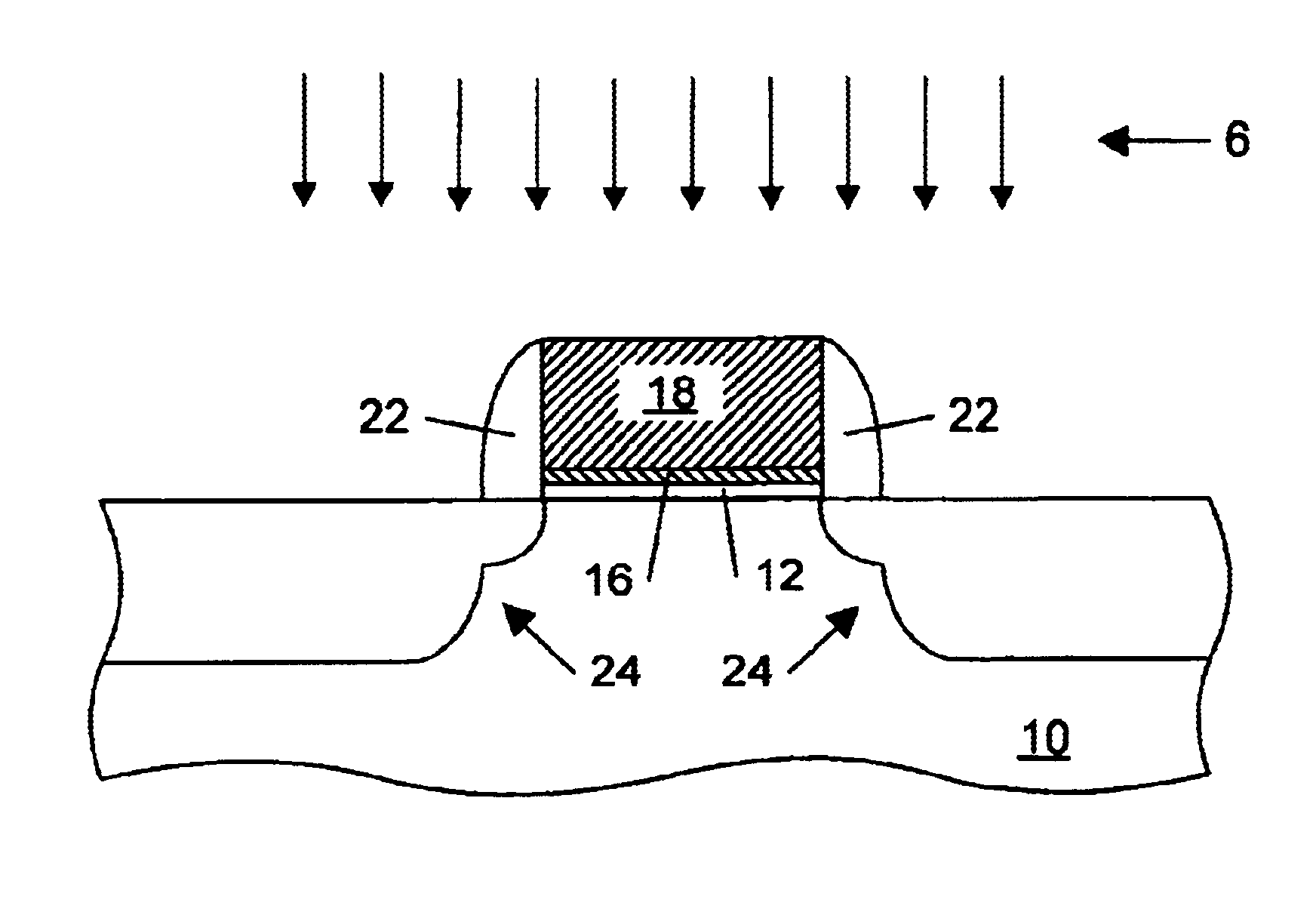
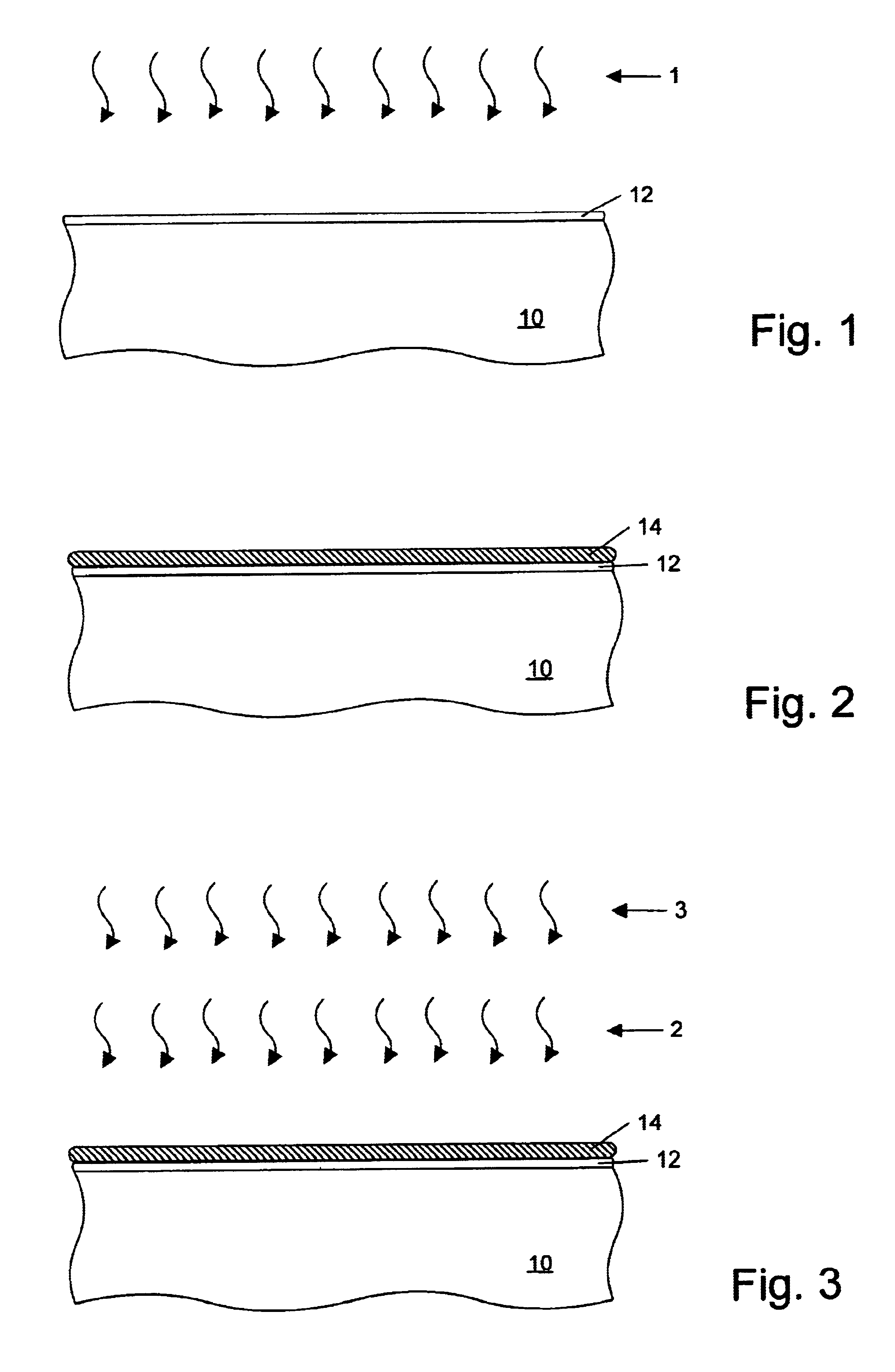
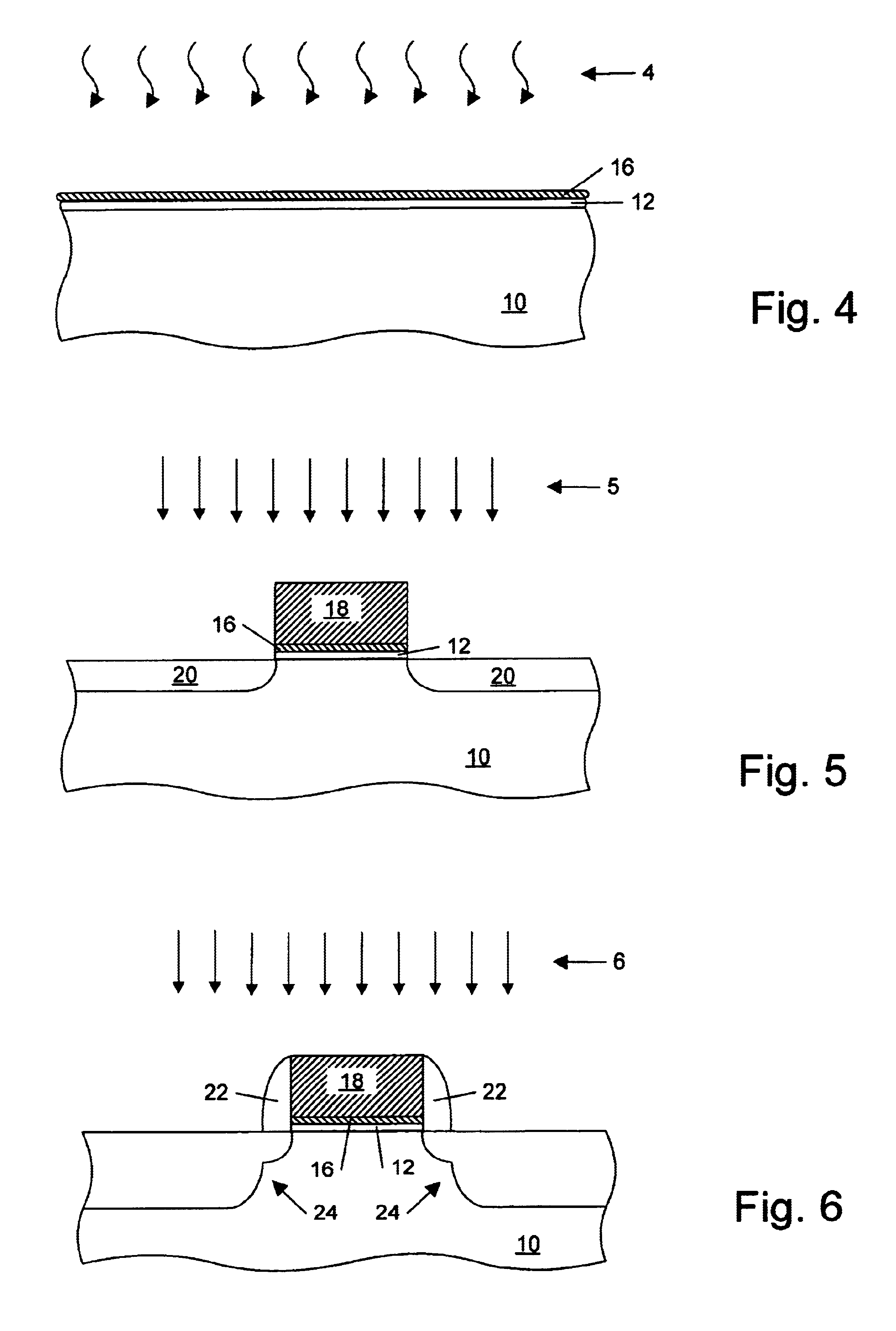
[0031]Turning to the drawings, FIG. 1 illustrates a partial cross-section of a semiconductor topography including an ultrathin (from about 4 angstroms to about 8 angstroms thick) nitrogen-containing oxide 12 formed upon a semiconductor substrate 10. Semiconductor substrate 10 is preferably silicon, and is doped either n-type (for producing a p-channel transistor) or p-type (for an n-channel transistor). More specifically, substrate 10 may be an epitaxial silicon layer grown on a monocrystalline silicon substrate, or an n-type or p-type well region formed in a monocrystalline silicon substrate. The method recited herein may also be suitable for other semiconductors, such as, for example, gallium arsenide. Although not shown, there may be dielectric isolation regions formed within substrate 10 to prevent electrical interaction between subsequently-formed semiconductor devices. Methods of forming the isolation regions may include dielectric deposition to fill trenches etched into the s...


PUM


Abstract

An ultrathin gate dielectric having a graded dielectric constant and a method for forming the same are provided. The gate dielectric is believed to allow enhanced performance of semiconductor devices including transistors and dual-gate memory cells. A thin nitrogen-containing oxide, preferably having a thickness of less than about 10 angstroms, is formed on a semiconductor substrate. A silicon nitride layer having a thickness of less than about 30 angstroms may be formed over the nitrogen-containing oxide. The oxide and nitride layers are annealed in ammonia and nitrous oxide ambients, and the nitride layer thickness is reduced using a flowing-gas etch process. The resulting two-layer gate dielectric is believed to provide increased capacitance as compared to a silicon dioxide dielectric while maintaining favorable interface properties with the underlying substrate. In an alternative embodiment, a different high dielectric constant material is substituted for the silicon nitride. Alternatively, both nitride and a different high dielectric constant material may be used so that a three-layer dielectric is formed.

Description

BACKGROUND OF THE INVENTION[0001]1. Field of the Invention[0002]This invention relates to integrated circuit fabrication and, more particularly, to a gate dielectric having a high dielectric constant and favorable interface properties with underlying semiconductor regions, and to a method for producing this gate dielectric by combining deposition, annealing, and etchback techniques.[0003]2. Description of the Relevant Art[0004]Fabrication of a metal-oxide-semiconductor (MOS) integrated circuit involves numerous processing steps. A gate dielectric, typically formed from silicon dioxide (“oxide”), is formed on a semiconductor substrate which is doped with either n-type or p-type impurities. For each MOS field effect transistor (MOSFET) being formed, a gate conductor is formed over the gate dielectric, and dopant impurities are introduced into the substrate to form a source and drain. A pervasive trend in modem integrated circuit manufacture is to produce transistors having feature siz...

Claims


Application Information

Patent Timeline
IPC IPC(8): H01L21/02H01L21/28H01L29/51H01L29/40H01L21/314
CPCH01L21/28185H01L21/28202H01L29/518H01L29/513H01L21/28194H01L29/517H01L21/3144H01L21/022
Inventor GARDNER, MARK I.KWONG, DIM-LEEFULFORD, JR., H. JIM
Owner ADVANCED MICRO DEVICES INC
Why Eureka
Try Eureka