In-situ toughening method for tough integrated Cu/Sn/Ag welding material

A welding material and physical technology, applied in welding/cutting medium/material, welding medium, welding equipment, etc., can solve the problems of low strength and plasticity, insufficient elasticity and plasticity, large amount of precious metal, etc., and achieve high temperature resistance reliability. Guaranteed, reduced soldering temperature, and simple preparation method

Active Publication Date: 2021-01-01
INST OF ELECTRICAL ENG CHINESE ACAD OF SCI
View PDF14 Cites 2 Cited by
  • Summary
  • Abstract
  • Description
  • Claims
  • Application Information

AI Technical Summary

Problems solved by technology

[0003] Typical "sandwich" metal structure-LT-TLPB is a high temperature resistant pure interfacial intermetallic compound (IMCs) joint, which is based on low melting point metals such as Sn and In in the middle layer, and Cu, Ni, Au, Zn, etc. in the surface layer The sandwich structure of high-melting-point metals uses the melting of low-melting-point metals to produce liquid-solid interdiffusion, and generates high-temperature-resistant IMCs as a welding technology for connecting joints. The thickness of the welding layer using this welding technology is generally less than 20 μm, which is not conducive to absorbing due to chips and The thermal stress generated by the adaptation of the thermal expansion coefficient of system materials such as substrates is difficult to meet the needs of high-reliability packaging of power electronic devices
Chinese patent CN100475996C discloses a composition, production method and components for high-temperature lead-free solder. The phase line is not lower than 262.5°C, and the liquidus line is not higher than 400°C. However, the strength and plasticity of the lead-free solder composition are low, and the solder paste made of ordinary solder paste for this solder has poor collapse resistance. , more tin beads and other defects are unfavorable for the industrialized production and promotion of the composition for lead-free solder
CN104476007A discloses a high-melting point lead-free halogen-free solder paste and its preparation method. The solder paste solder alloy has a solidus temperature higher than 260°C and has the advantages of high strength, high plasticity, and strong fatigue resistance. Soldering paste has complex process, easy to pollute the chamber, and the porosity of the prepared joints is large; Chinese patent CN101234456A discloses a tin-silver-gold lead-free soldering material and its preparation method. Its melting temperature can reach 300 ° C, wet Excellent electrical and electrical properties, good welding effect, can replace the traditional Sn-95%Pb solder alloy
The amount of precious metal is large, the cost is high, and the welding temperature is high; Chinese patent CN104588906A discloses a Sn-Cu high-temperature lead-free solder paste and its preparation method and use method. The shear strength is high, but the elasticity and plasticity are insufficient, and this technology still uses solder paste, which needs to adopt a screen printing process that is prone to pollution; due to the welding process, the solder material cannot be wetted and spread, so the solder paste is left behind after volatilization Large-area holes and loose joints affect thermal conductivity and reliability; Chinese patent CN103753049A discloses a Cu / Sn solder sheet with high temperature resistance, but Cu 3 The Kirkendall voids produced by the Sn generation process are high, and the thermal and electrical conductivity are affected. In addition, the elastic modulus of the Cu particles is high, the joint toughness is insufficient, and the reliability at high temperatures is difficult to meet the requirements.

Method used


Image

  • In-situ toughening method for tough integrated Cu/Sn/Ag welding material
  • In-situ toughening method for tough integrated Cu/Sn/Ag welding material
  • In-situ toughening method for tough integrated Cu/Sn/Ag welding material

Examples


Embodiment 1

[0048] Copper powder with a particle size of 5-10 μm and 10-15 μm is used to prepare the electroplating Sn coating and the physical vapor deposition Ag coating in sequence, and the particle size is graded according to the ratio of 3:2, and the graded powder is placed in a high-speed ball mill. , mechanically mixed at a rate of 100r / min for 1h to obtain a homogeneously mixed composite powder.

[0049] Weigh 0.13g of the above-mentioned mixed powder, perform high-pressure tablet pressing on a press with a pressure of 10MPa, and hold a constant pressure for 10 minutes to obtain a solder sheet with a thickness of 389μm;

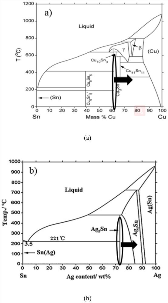
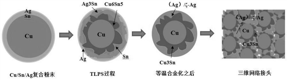
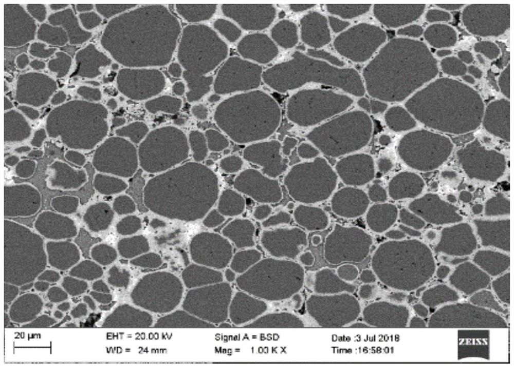
[0050] Sinter the solder sheet prepared above in a vacuum soldering furnace at 250°C, the low-temperature Sn melts and instantly reacts with Ag and Cu to form Cu through solid-liquid diffusion reaction. 6 sn 5 with Ag 3 Sn interface intermetallic compound, after 8 minutes of reflux, the Sn coating is completely transformed into an interfacial intermetallic comp...

Embodiment 2

[0052] Copper powders with a particle size of 5-10 μm and 15-20 μm were used to prepare Sn electroplating and Ag coatings by physical vapor deposition in sequence, and the particle size was graded according to the ratio of 3:1, and the graded powder was placed in a high-speed ball mill. Mix mechanically at a rate of 200r / min for 2h to obtain a uniformly mixed composite powder.

[0053] Weigh 0.13g of the above-mentioned mixed powder, perform high-pressure tablet pressing on a press with a pressure of 15 MPa, and hold a constant pressure for 10 minutes to obtain a solder sheet with a thickness of 380 μm;

[0054] Sinter the solder sheet prepared above in a vacuum soldering furnace at 250°C, the low-temperature Sn melts and instantly reacts with Ag and Cu to form Cu through solid-liquid diffusion reaction. 6 sn 5 with Ag 3 Sn interface intermetallic compound, after 6 minutes of reflow, the Sn coating is completely transformed into an interfacial intermetallic compound, and the...

Embodiment 3

[0056] Copper powders with a particle size of 10-15 μm and 15-20 μm were used to prepare Sn electroplating and Ag coatings by physical vapor deposition, respectively, and the particle size was graded according to the ratio of 2:1. The graded powder was placed in a high-speed ball mill. Mix mechanically for 2 hours at a rate of 300 r / min to obtain a uniformly mixed composite powder.

[0057] Weigh 0.13g of the above-mentioned mixed powder, perform high-pressure tablet pressing on a press with a pressure of 20 MPa, and hold a constant pressure for 10 minutes to obtain a solder sheet with a thickness of 395 μm;

[0058] Sinter the solder sheet prepared above in a vacuum soldering furnace at 250°C, the low-temperature Sn melts and instantly reacts with Ag and Cu to form Cu through solid-liquid diffusion reaction. 6 sn 5 with Ag 3 Sn interface intermetallic compound, after 8 minutes of reflow, the Sn coating is completely transformed into an interfacial intermetallic compound, an...


PUM

PropertyMeasurementUnit
thicknessaaaaaaaaaa
shear strengthaaaaaaaaaa
elastic modulusaaaaaaaaaa

Abstract

The invention relates to an in-situ toughening method for a tough integrated Cu/Sn/Ag welding material. The method comprises the steps of step (1), uniformly electroplating a 2-3 [mu]m Sn plating layer on copper particles with different particle sizes, then, physically and uniformly depositing a 1 [mu]m Ag layer on the surface of Cu/Sn powder to obtain Cu/Sn/Ag powder; step (2), proportioning theCu/Sn/Ag powder prepared in the step (1), placing the Cu/Sn/Ag powder in a mixer, and performing mechanical mixing for 1 to 2 hours at the speed of 100 to 300 r/min to obtain powder with uniformly mixed particle sizes; step (3), performing pressure forming on the powder prepared in the step (2) on a high-pressure tablet press with the pressure range of 10 MPa to 30 MPa to obtain a Cu/Sn/Ag composite preformed welding chip with the thickness of 100 [mu]m to 400 [mu]m; and step (4), performing low-temperature transient liquid-phase diffusion welding on the composite preformed welding chip, and enabling Sn with a low melting point to be completely converted into a high-temperature-resistant Cu3Sn and Ag3Sn interface intermetallic compound through simultaneous diffusion reaction of Sn and Cu and simultaneous diffusion reaction of Sn and Ag at a point below the melting point of Sn, so as to prepare a Cu3Sn/Ag3Sn-clad Cu particle three-dimensional network structure joint.

Description

technical field [0001] The invention relates to a lead-free solder preform of a high-temperature-resistant three-dimensional network joint for power electronic packaging and an in-situ toughening method for a strong and tough integrated Cu / Sn / Ag welding material. Background technique [0002] Power electronics (or power) modules are important energy conversion and control devices, widely used in aerospace, rail transit, advanced energy, electric vehicles, oil drilling, major and advanced equipment manufacturing, frontier scientific research and other fields. With the development of electronic products in the direction of miniaturization, high density, and high power, and the industrial application of third-generation semiconductor devices represented by SiC, power electronic modules are facing the challenges of higher temperature tolerance and higher reliability. The comprehensive lead-free module is gradually put on the agenda, and the corresponding lead-free packaging join...

Claims


Application Information

Patent Timeline
Patent Type & Authority Applications(China)
IPC IPC(8): B22F1/02B22F3/02B22F5/00B23K20/00B23K20/26B23K35/40C23C14/16C23C14/34C23C28/02C25D3/30
CPCB22F3/02B22F5/00B23K35/40B23K20/00B23K20/26C25D3/30C23C14/165C23C14/34C23C28/023B22F1/17
Inventor 徐红艳徐菊
Owner INST OF ELECTRICAL ENG CHINESE ACAD OF SCI
Why Eureka
Try Eureka