A preparation method and application of silicon-based microneedles by metal-assisted wet etching

A wet etching, metal-assisted technology, applied in the direction of microneedle, metal material coating process, needle head, etc., can solve problems such as unfavorable large-scale manufacturing, cumbersome process, unfavorable commercial application, etc., and achieve good linear response, Simple process and controllable position of microneedles

Active Publication Date: 2022-08-09
UNIV OF SCI & TECH OF CHINA
View PDF11 Cites 0 Cited by
  • Summary
  • Abstract
  • Description
  • Claims
  • Application Information

AI Technical Summary

Problems solved by technology

[0003] At present, in terms of materials, microneedles can be divided into metal microneedles, silicon-based microneedles, polymer microneedles, etc., but because of their own size, the processing process is more complicated and difficult
Metal microneedles are mostly made by CNC processing, or making related molds, which is complicated to operate, and if applied to large-scale production, the cost is high; polymer microneedles generally need molds to be manufactured for drug delivery and treatment, and cannot be long-lasting. Time to detect whether the indicators of the human body are normal; the manufacturing process of silicon-based microneedles can also be divided into two categories: the first is dry etching, which needs to grow a layer of silicon oxide or silicon nitride as a mask, and then pattern it Processing, reaction-coupled plasma etching can etch micro-pillars with better verticality, and then use silicon etching solution to etch the micro-pillars to form tips. The above process requires a large number of instruments and equipment, and the cost is too high, and the manufacturing efficiency is low; The second method uses anisotropic etching of silicon under alkaline conditions. This method requires the use of low-pressure chemical vapor deposition to form a mask, and then the silicon wafer is soaked in potassium hydroxide solution for a long time to form a large area of ​​pyramid-shaped microstructure. Needles, but the cost of forming a mask is high, and the etching time of potassium hydroxide is too long (usually it takes eight to nine hours to etch a pyramid height of more than 200 microns at room temperature), which is not conducive to large-scale manufacturing and commercial application
[0004] At present, the manufacturing methods of silicon-based microneedles generally require chemical vapor deposition, reactive ion etching, reaction-coupled plasma etching and other more complicated process steps. The process is cumbersome, the processing cost is high, and the manufacturing cycle time is long.
In large-scale array manufacturing, due to the complexity of device manufacturing process steps, there are few cases, and it is difficult to achieve commercial application

Method used


Image

  • A preparation method and application of silicon-based microneedles by metal-assisted wet etching
  • A preparation method and application of silicon-based microneedles by metal-assisted wet etching
  • A preparation method and application of silicon-based microneedles by metal-assisted wet etching

Examples


preparation example Construction

[0031] The invention provides a preparation method for preparing silicon-based microneedles by metal-assisted wet etching, comprising the following steps:

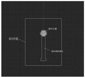
[0032] The surface of the pretreated silicon wafer is coated with photoresist for patterning to obtain a sample;

[0033] depositing the sample in a mixed solution of silver nitrate-hydrofluoric acid-ultrapure water to obtain a deposited silicon wafer;

[0034] The deposited silicon wafer is etched in a hydrofluoric acid-hydrogen peroxide mixed solution, washed and soaked in a piranha solution, and then silicon nanowires are removed to obtain silicon-based microneedles.

[0035] The present invention proposes a completely new process step that solves the problems of cost, instrumentation and operation. Using the principle of metal-assisted wet etching combined with semiconductor technology, the requirements for silicon-based samples are very low, and the requirements for the experimental environment are not high. The requ...

Embodiment 1

[0054] A clean and flat silicon-based substrate is selected. The present invention selects a (100) crystal-oriented silicon wafer. There is no requirement for doping. The silicon wafer needs to be soaked and cleaned with acetone for 5 minutes, and then rinsed with ultrapure water for 1 minute. Put the silicon wafer into the piranha solution (H 2 SO 4 :H 2 O 2 = 3:1 volume ratio) for 10 minutes, and it is necessary to ensure that the temperature of the piranha solution is at room temperature. This step is to form an oxide layer. The silicon wafer with the oxide layer was washed with ultrapure water for 1 min, and then immersed in a 5% hydrofluoric acid solution for 5 min to remove the oxide layer to expose a new silicon interface, rinsed with ultrapure water for 1 min and dried with nitrogen.

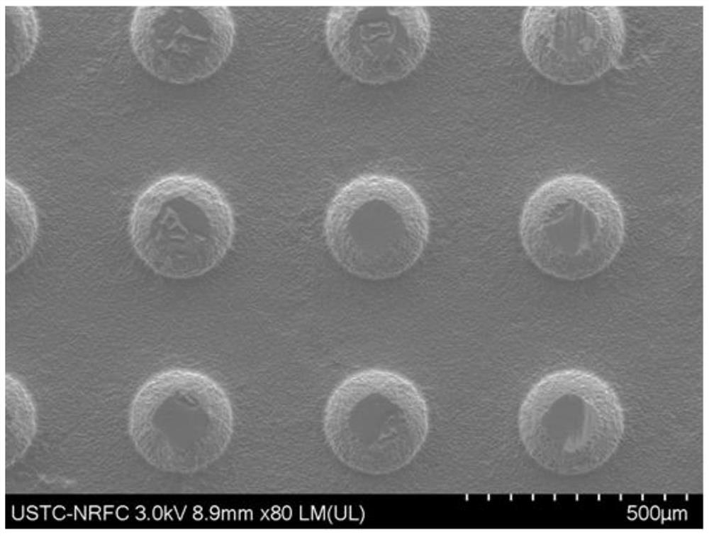
[0055] The pattern of the photolithography mask is a circle with a diameter of 250μm and an array with a spacing of 200um outside the circle. The uniform photoresist (S1813) is applie...

Embodiment 2

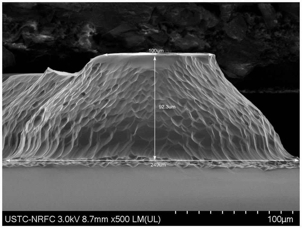
[0061] The difference from Example 1 is that it was placed in the etching solution to etch for 8 minutes.

[0062] The height of the silicon-based microneedles prepared in Example 2 is about 110 microns.


PUM

PropertyMeasurementUnit
heightaaaaaaaaaa
heightaaaaaaaaaa
heightaaaaaaaaaa

Abstract

The present invention provides a preparation method to prepare silicon -based microneedles with metal auxiliary wet etching, including: the pre -processing silicon wafer surface is applied to the graphic processing to obtain the sample;Fluoric acid 纯 ultra -pure water hybrid solution is deposited to obtain sedimentary silicon wafers; the sedimentary silicon wafers are carved in the hydrogen hydrogen peroxide hydrogen peroxide mixed solution, soaked in the ingredients solution after washing, and then removed the silicon nano wire., Get the silicon -based microneedle.The method provided by the present invention only needs to be treated with a simple map with photoresist, and then the metal auxiliary wetting method is used to etched out large -sized microcliclement under acidic conditions.The etching time is short, the process is simple, and the effect is significant.The height of the silicon -based microneedle is 90 to 137 microns; the prepared sensors have a good linear response to hydrogen peroxide, and the response current is large. It can detect changes in the concentration of hydrogen peroxide at no less than 4 hours.

Description

technical field [0001] The invention belongs to the technical field of microneedle preparation, and in particular relates to a preparation method and application of silicon-based microneedles prepared by metal-assisted wet etching. Background technique [0002] Effective medical management also relies on new diagnostic methods that enable rapid, sensitive, and accurate detection and monitoring of related diseases of social concern. This is one of the main reasons why biomarker and biosensor research continues to evolve. In this framework, the degree of innovation of standard sensing technologies is very important despite the use of transformation methods. Several optical techniques such as surface plasmon resonance, surface-enhanced Raman spectroscopy, fluorescence, and electrochemical techniques based on voltammetry and impedance spectroscopy have been demonstrated for highly sensitive target analytes. Among them, electrochemical devices in electrochemical technology gene...

Claims


Application Information

Patent Timeline
Patent Type & Authority Patents(China)
IPC IPC(8): A61M37/00C23F1/24C23F1/02C23C18/42
CPCA61M37/0015C23C18/42A61M2037/0053
Inventor 周成刚马圆圆魏钰陈琳
Owner UNIV OF SCI & TECH OF CHINA
Why Eureka
Try Eureka