Minisize solid silicon needle array chip and its preparation method and use

A needle array, solid technology, applied in the direction of microneedles, needles, other medical devices, etc.

Active Publication Date: 2005-01-26
SUZHOU NANOMED BIOMED CO LTD
View PDF1 Cites 27 Cited by
  • Summary
  • Abstract
  • Description
  • Claims
  • Application Information

AI Technical Summary

Problems solved by technology

Specifically, the method uses photolithography to form patterns on the surface of single crystal silicon, and then uses deep ion reactive etching technology to form conical microneedles such as figure 1 , but the microneedles made by this method are too sharp, and about 5% of them break during use

Method used


Image

  • Minisize solid silicon needle array chip and its preparation method and use
  • Minisize solid silicon needle array chip and its preparation method and use
  • Minisize solid silicon needle array chip and its preparation method and use

Examples


Embodiment 1

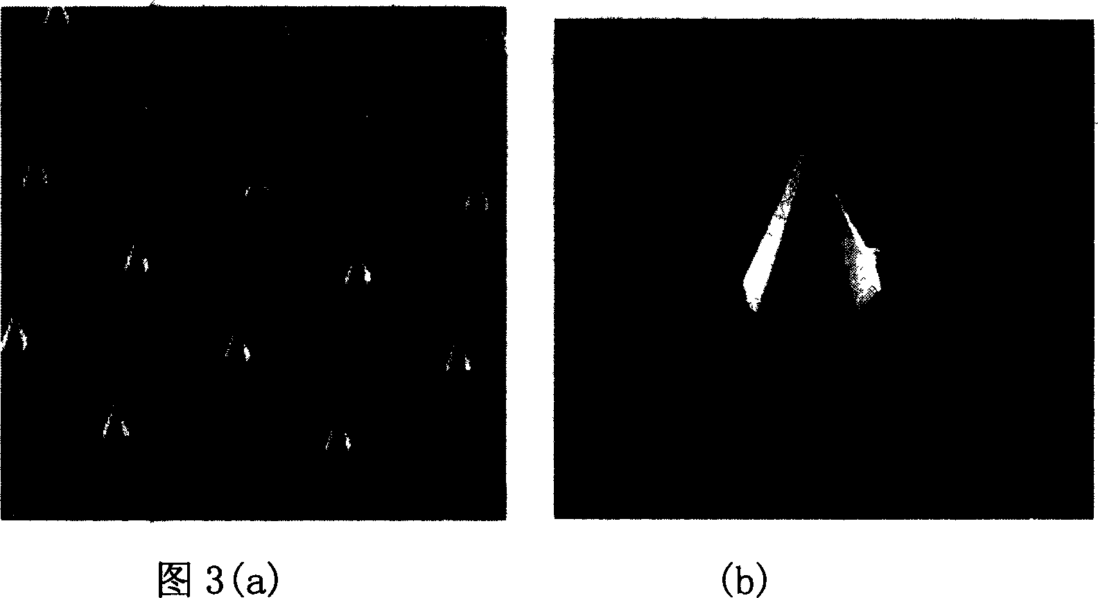
[0084] Embodiment 1: the making of tapered micro-silicon needle

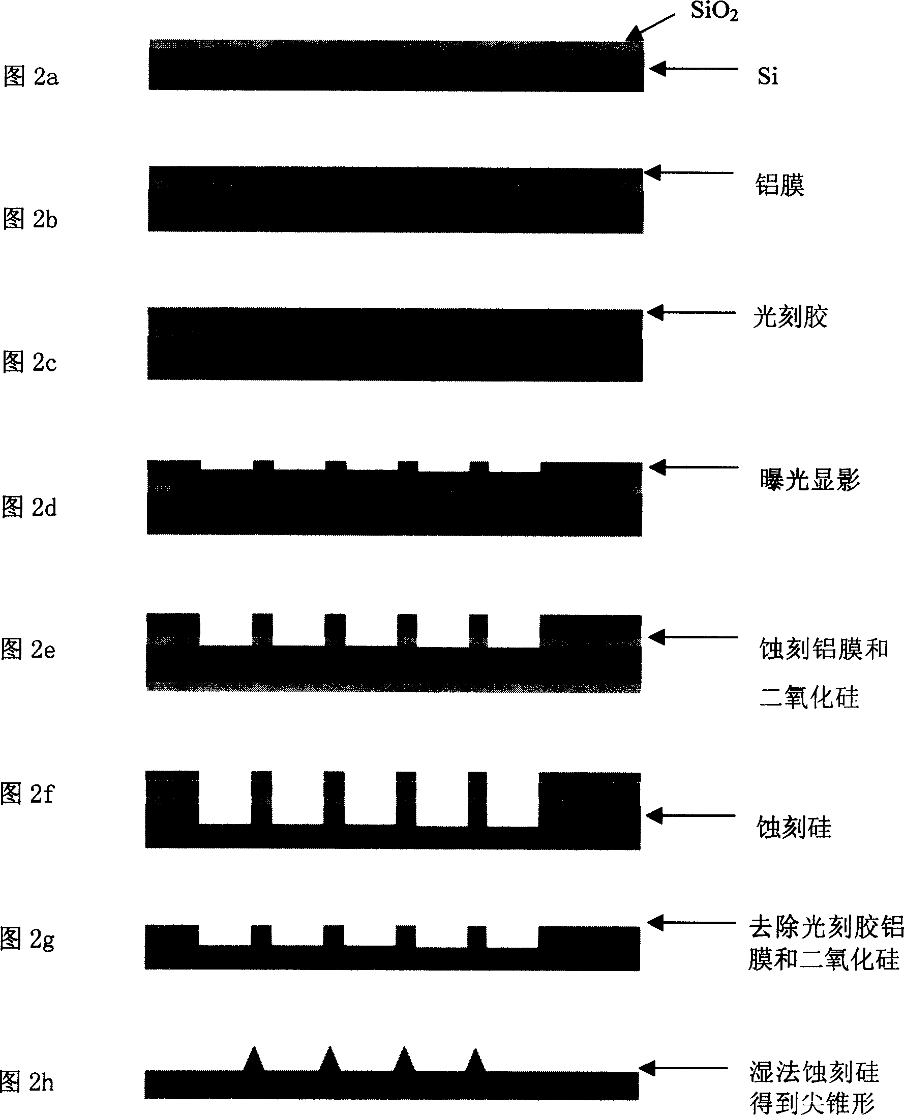
[0085] Basic process flow: Single-sided polishing of single crystal silicon wafer → growth of a layer of SiO 2 →Deposit metal film→Glue coating→Photolithography to obtain solid microneedle pattern→Reactive ion etching (RIE) removes metal film and SiO not protected by photoresist 2 Partial→anisotropic deep reactive ion etching (DRIE) to obtain microcylindrical arrays→wet etching to obtain solid microneedles.

[0086] Single-sided polished single crystal silicon type, 500 microns thick as raw material. The monocrystalline silicon was first cleaned with a cleaning solution containing 5 parts of deionized water, 1 part of 30wt% hydrogen peroxide and 1 part of 30wt% ammonia water at a temperature close to 80 degrees, and then dried at 150 degrees for 10 minutes. A silicon dioxide layer with a thickness of about 1 micron is grown on both sides of the single crystal silicon type through thermal oxidation at 900-11...

Embodiment 2

[0087] Embodiment 2: the making of nail type miniature solid silicon needle

[0088] Single-sided polished single crystal silicon type, 500 microns thick as raw material. The monocrystalline silicon was first cleaned with a cleaning solution containing 5 parts of deionized water, 1 part of 30wt% hydrogen peroxide and 1 part of 30wt% ammonia water at a temperature close to 80 degrees, and then dried at 150 degrees for 10 minutes. A silicon dioxide layer with a thickness of about 1.5 microns is grown and formed on the surface of single crystal silicon through high temperature thermal oxidation at 900-1100 ° C; a uniform layer of 1-2 microns is coated on the silicon dioxide film by the spin coating method Thick Shipley 1818 photoresist, pre-baked (soft baked) at 90 degrees for 5 minutes, formed a 80×80 array in a unit of 1 square centimeter, with a diameter of 100 microns and a solid circle mask with a pitch of 200 microns film (quartz glass is used in the semiconductor standa...

Embodiment 3

[0089] Embodiment 3: the making of tapered micro-silicon needle

[0090] Basic process flow: Double-sided polishing of single crystal silicon wafer → growth of a layer of SiO 2 →Deposit metal film→Glue coating→Photolithography to obtain solid microneedle pattern→Hydrochloric acid solution and a mixture of ammonium fluoride and hydrofluoric acid to remove the metal film and SiO not protected by photoresist 2 Partial→anisotropic deep reactive ion etching (DRIE) to obtain microcylindrical arrays→wet etching to obtain solid microneedles.

[0091] Double-sided polished single crystal silicon type, 500 microns thick as raw material. The single crystal silicon is first cleaned with a cleaning solution containing 5 parts of deionized water, 1 part of 30wt% hydrogen peroxide and 1 part of 30wt% ammonia water at a temperature close to 80 degrees, and then dried at 120 degrees for 10 minutes. A silicon dioxide layer with a thickness of about 1 micron is grown on both sides of the sin...


PUM

PropertyMeasurementUnit
diameteraaaaaaaaaa
diameteraaaaaaaaaa
heightaaaaaaaaaa

Abstract

The invention belongs to a transdermal drug releasing device field. It relates in particular to a preparing method and usage of the minitype solid silicon pin array chip by monocrystalline silicon and Microelectromechanical systems(MEMS) technology. The minitype solid silicon pin array chip is processed by the adoption of photoengraving, wet etching, plasma dry etching, filming and other MEMS technologies. A side groove opens on the side of the mini pins, one or a plurality of drug storage pool being manufactured on the back of the solid mini pins by the combined utilization of double face alignment light photo technology, the drug dosage can be increased by the connection of the drug storage pool and the solid mini pin surface. The present invention has simple process and durable solid mini pins, being suitable for transdermal drug release of bio drug with macromolecules in particular.

Description

technical field [0001] The invention belongs to the field of transdermal drug release devices, in particular to a micro-solid silicon needle array chip made of single crystal silicon, and a method for manufacturing a micro-solid silicon needle array chip and a micro-solid silicon needle array chip using micro-electromechanical processing (MEMS) technology. The use of silicon needle array chips. Background technique [0002] In general, drugs can be made into a variety of formulations, so there can be different routes and methods of administration. The route and method of administration affect the drug metabolism, thereby affecting the curative effect. [0003] Most drugs are currently administered orally in the form of tablets and capsules. However, due to the degradation of drugs in the gastrointestinal tract and the first-pass effect of the liver, many orally administered drugs are mostly or completely ineffective before reaching the site of actio...

Claims


Application Information

Patent Timeline
Patent Type & Authority Applications(China)
IPC IPC(8): A61M37/00
CPCA61M37/0015A61M2037/0053
Inventor 徐百高云华
Owner SUZHOU NANOMED BIOMED CO LTD
Why Eureka
Try Eureka