

Plasma ashing process
- Summary
- Abstract
- Description
- Claims
- Application Information
AI Technical Summary
Benefits of technology
Problems solved by technology
Method used
Image

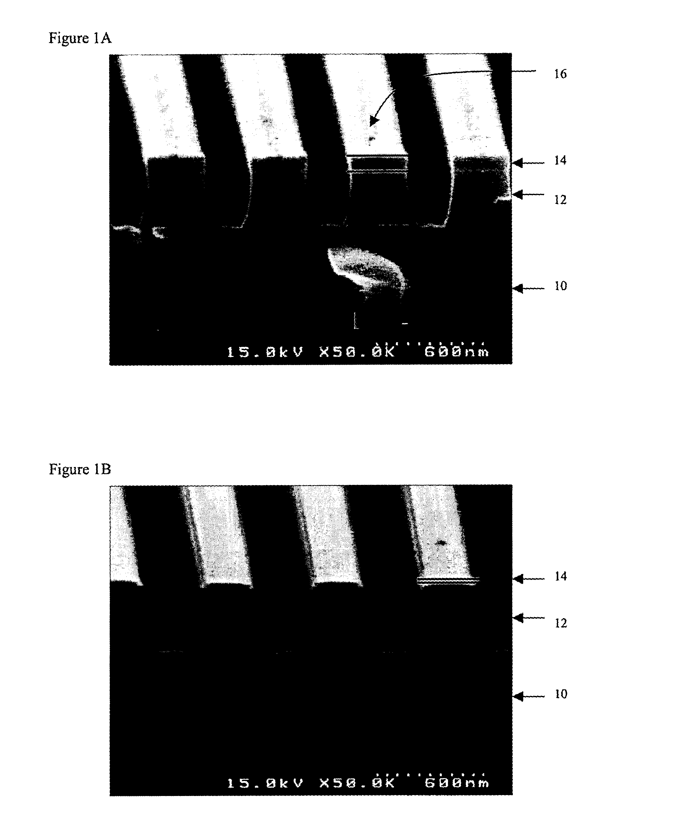
Examples
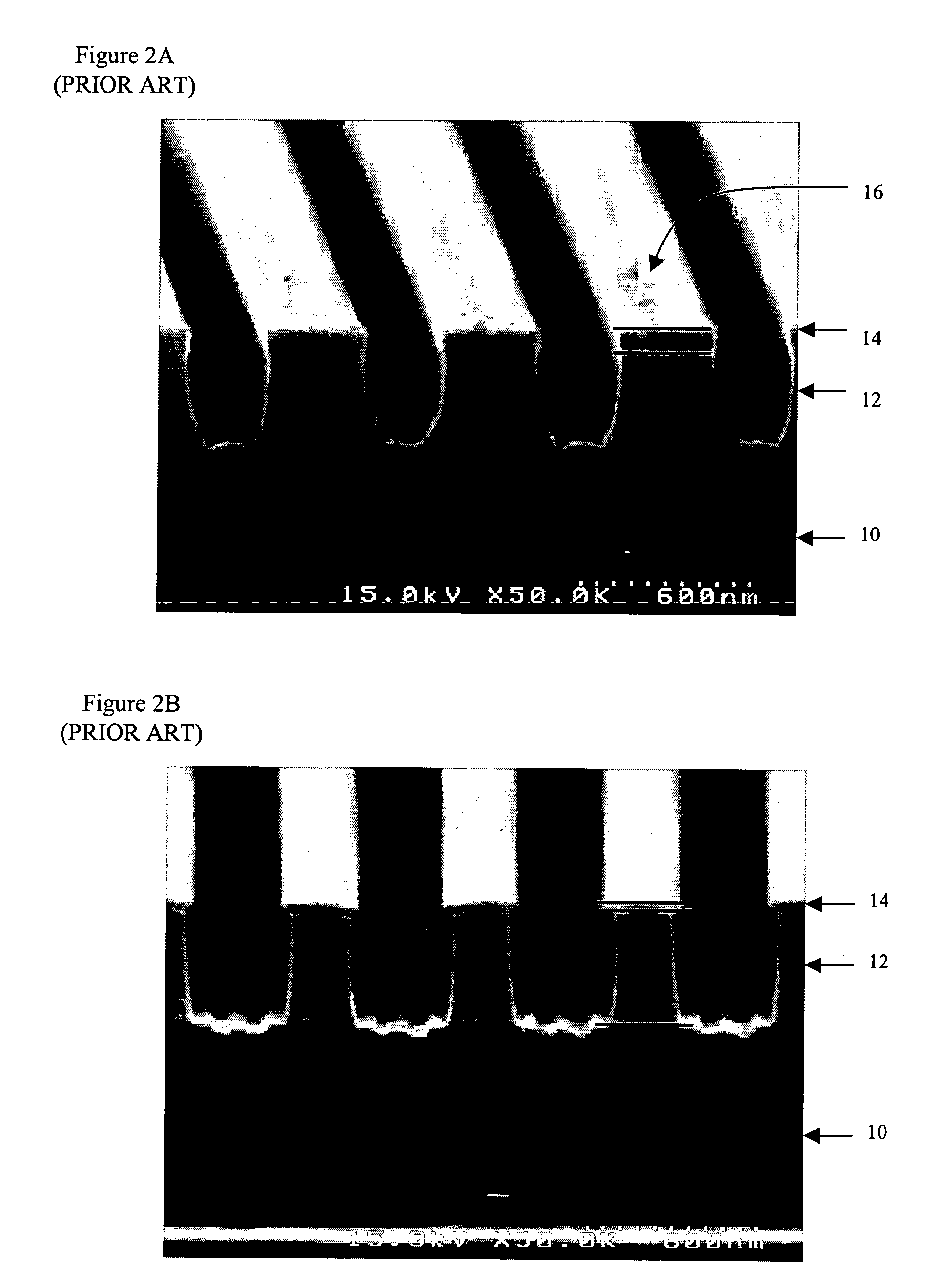
example 2
[0048] In this example, the substrates were prepared in accordance with Example 1 and exposed to a conventional ashing plasma process. The plasma gas mixture included nitrogen gas in place of the helium gas and at the same volume percentage. All other conditions were identical to that in Example 1. The process conditions are shown in Table II.
2TABLE II Nitrogen-containing Plasma Time Pressure Power 5% H.sub.2 / N.sub.2 CF.sub.4 Step (min.) (torr) (W) Temp (.degree. C.) (sccm) (sccm) 1 25 1.5 Off 370 5000 50 2 20 1.5 1500 370 5000 50
[0049] As shown in FIG. 2A, scanning electron microscopy of substrates ashed with the nitrogen-containing plasma yielded results similar to the nitrogen-free plasma process of Example 1. A comparison of FIGS. 1A and 2A show similar etch profiles. However, as shown in FIG. 2B, exposing the ashed wafers to the same wet clean process used in Example 1 resulted in significant CD loss of the low k dielectric layer 12. The wet clean process clearly removed signif...
example 3
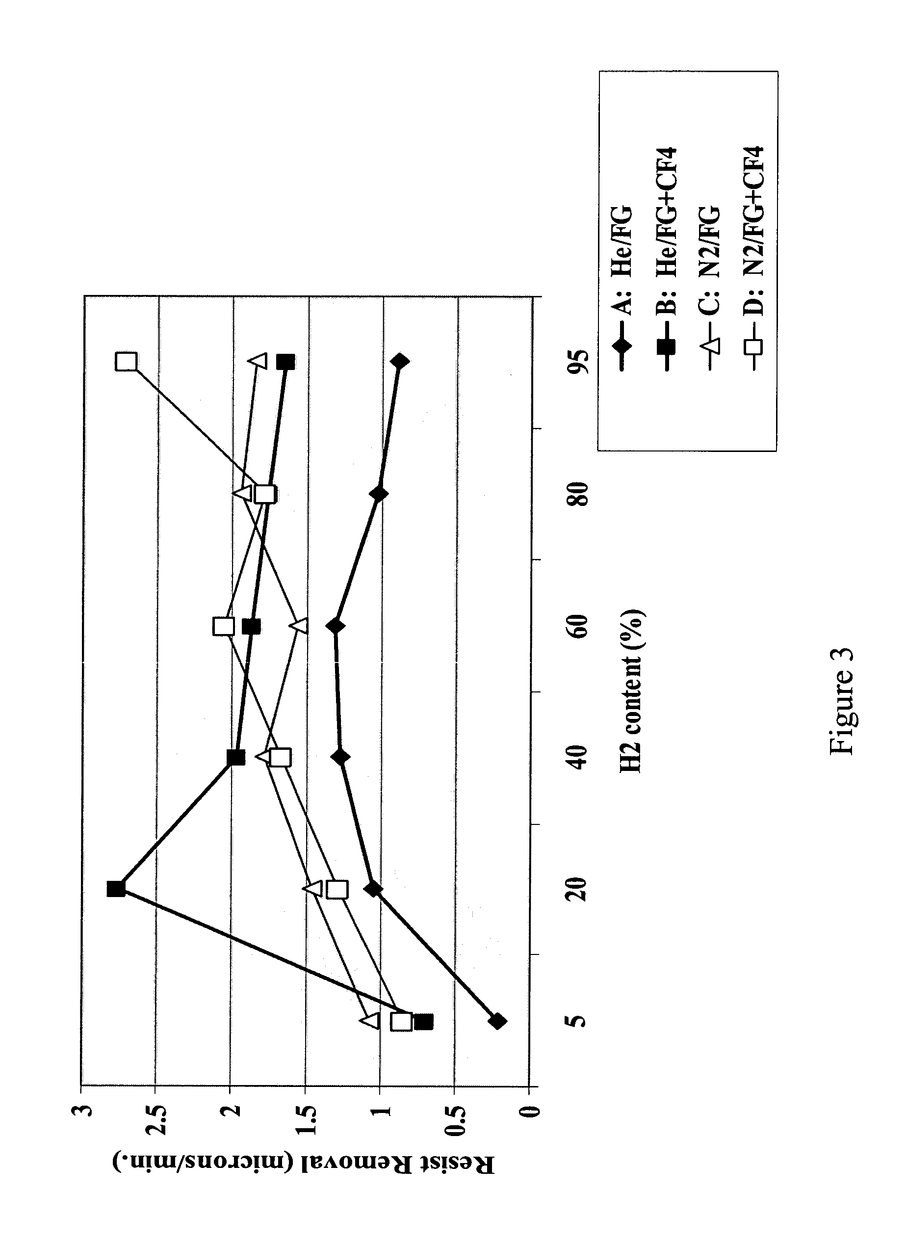
[0050] In this example, the rate of photoresist removal was monitored as a function of the percentage of hydrogen gas in the plasma. Substrates were coated with a thick layer of photoresist and exposed to one of four different plasmas (A-D) in a Fusion Gemini ES3 plasma asher. The process conditions and flow rates were held constant for each wafer set. The photoresist thickness was conventionally measured by ellipsometry before and after processing in order to determine the removal rate. As shown in Table III, the substrates were exposed to: A. a nitrogen-free plasma, B. a nitrogen-free plasma with tetrafluoromethane (CF.sub.4), C. a nitrogen-containing plasma and D. a nitrogen-containing plasma with CF.sub.4. The percentage of hydrogen in the plasma gas mixture was varied as a percentage of the total volume of the hydrogen gas mixture. The results are graphically shown in FIG. 3.
3TABLE III Plasma Gas Compositions Hydrogen / Nitrogen (FORMING GAS) Hydrogen / Helium CF.sub.4 PLASMA flow ...
example 4
[0052] In this example, the effect of nitrogen and oxygen impurity levels in an oxygen and nitrogen free plasma ashing process was examined. In particular, substrates containing a porous low k carbon containing dielectric were processed at various process temperatures and various impurity levels. Thickness loss of the low k dielectric layer was measured subsequent to a 30 second rinse in 100:1 dilute HF mixture.
[0053] FIG. 5 graphically illustrates the loss of low k dielectric for a hydrogen / helium plasma containing various nitrogen levels (parts per million) at ashing temperatures of 270, 300, and 330.degree. C. Surprisingly, low k dielectric loss was less than 50 angstroms at a N.sub.2 impurity level of about 50 ppm and an ashing process temperature of 270.degree. C. Similar results were obtained with oxygen at an impurity level of 20 ppm. Previous experiments as demonstrated in Example 3 above suggested that damage would occur to the low k dielectric material in the presence of s...
PUM
| Property | Measurement | Unit |
|---|---|---|
| Fraction | aaaaa | aaaaa |
| Fraction | aaaaa | aaaaa |
| Fraction | aaaaa | aaaaa |
Abstract
Description
Claims
Application Information