Polishing composition for semiconductor wafer

a technology of polishing composition and semiconductor wafer, which is applied in the direction of lapping machines, manufacturing tools, other chemical processes, etc., can solve the problems of affecting the yield and quality of products, affecting the quality of products, and causing minute crushes, etc., to prevent over-etching, maintain adequate polishing ability, and great polishing ability

Inactive Publication Date: 2010-07-01
NIPPON CHECMICAL IND CO LTD +1
View PDF2 Cites 21 Cited by
  • Summary
  • Abstract
  • Description
  • Claims
  • Application Information

AI Technical Summary

Benefits of technology

[0036]By using the polishing composition of present invention, one can obtain excellent effect in preventing over etching in polishing of a semiconductor wafer and the like. “Over etching” is a phenomenon that causes by corrosion of a wiring metal which results formation of recesses during polishing process of the wiring metal, an insulation film or a barrier film. Over etching occurs when a balance of corrosive speed between a mechanical polishing action by polishing particles and a corrosive action by alkaline component is broken. Over etching is recognized as a ground of defective products such as corrosive pits, wiring corrosions or key holes of tungsten wiring. Further, since said polishing composition does not contain alkali metals, problems such as remaining of polishing particles or dispersion of alkali metal to wiring layer can be prevented. So, the present invention has great influence to the relating field.
[0037]As mentioned above, nitrogen containing basic compounds are the useful agents in metal polishing and are disclosed in many Patent Documents. On the other hand, polishing composition for semiconductor wafer polishing comprising, colloidal silica prepared from an active silicic acid aqueous solution obtained by removal of alkali from alkali silicate and at least one nitrogen containing basic compound selected from a group consisting of ethylenediamine, diethylenediamine, imidazole, methylimidazole, piperidine, morpholine, arginine, and hydrazine, is a new invention by the inventors of the present invention. And the fact that said colloidal silica can display great polishing ability while polishing a subject such as silicon wafer or the like is first shown in the present invention. Said polishing composition of the present invention can prevent over etching according to its close-neutral pH in spite of the alkali amount, can keep adequate polishing ability according to nonspherical shape of silica, and can keep the polishing ability according to existence of buffer solution.
[0038]Ethylenediamine is a strong base whose pKa is of about 9.9 and a pH of a 1% aqueous solution is about 11.8. There are two sorts of ethylenediamine: ethylenediamine anhydride and ethylenediamine mono hydrate. Ethylenediamine mono hydrate is preferred because it is less dangerous agent. Another name of diethylenediamine is piperazine and is also known as hexahydropyrazine or diethyleneimine. There are two sorts of diethylenediamine: diethylenediamine anhydride and diethylenediamine hexahydrate. Diethylenediamine hexahydrate is easier to use. Diethylenediamine is a strong base whose pKa is about 9.8 and a pH of a 1% aqueous solution is about 11.5. Imidazole is a weak base whose pKa is about 6.9 and a pH of a 1% aqueous solution is about 10.2. 2-methylimidazole is a weak base whose pKa is about 7.8 and a pH of a 1% aqueous solution is about 10.7. 4-methylimidazole can also be used instead of 2-methylimidazole. Other names of piperidine are hexahydropyridine and pentamethyleneimine. Piperidine is a strong alkali whose pKa is about 11.1 and a pH of a 1% aqueous solution is about 12.3. Morpholine is a slightly weak base whose pKa is about 8.4 and a pH of a 1% aqueous solution is about 10.8. Arginine is one of amino acids which also known as 5-guadidino-2-amino pentanoic acid and is a base whose pKa is about 12.5 and a pH of a 1% aqueous solution is about 10.5 because it possesses a carboxy group. Although each of D-, L- or DL-arginine can be used, L-arginine is preferably used among three because of low price. There are two sorts of hydrazine: hydrazine anhydrous and hydrazine monohydrate (also known as hydrohydrazine or hydrazine hydrate). Hydrazine monohydrate is preferred because it is less dangerous agent. Hydrazine is a strong reducing agent, however, as a base, it is a weak base whose pKa is about 8.1 and a pH of a 1% aqueous solution is about 9.9.
[0039]It is desirable that any kind of above mentioned nitrogen containing basic compounds do not contain alkali metals. Since any kind of said nitrogen containing basic compounds except arginine has strong irritative feature, toxicity, and corrosive feature, it is desirable to be used as an aqueous solution of about 10% concentration.
[0040]Above mentioned nitrogen containing basic compounds act as a polymerization catalyst of silica of an active silicic acid aqueous solution due to its basic feature. That is, colloidal particles can be obtained by heating the active silicic acid aqueous solution after alkalizing the solution by adding said nitrogen containing basic compounds. In the meanwhile, said nitrogen containing basic compounds affect particle form at a growing process of colloidal particles. Said nitrogen containing basic compounds bond with or adsorbs to surfaces of silica particles in the growing process and inhibits growing of particles at bonded parts and disturbs spherical growing of particles.
[0041]In the present invention, for the purpose of maintaining a stable polishing ability at actual polishing processes, it is desirable to maintain a solution at a pH of 8.5 to 11.0 at 25° C. When the pH is lower than 8.5, polishing rate becomes slow and is out of practical use. Further, when the pH is higher than 11.0, the solution over etches nonpolishing parts of a wafer and deteriorates a flatness of the wafer and is also out of practical use.

Problems solved by technology

If outermost periphery edge of the wafer is unevenly structured at the transportation, minute crushes are caused at the edge part of the wafer when the wafer collides with a transporting device and fine particles will arise.
The fine particles arisen will scatter and contaminate the precisely processed wafer surface, and affect seriously on the yield and the quality of products.
Especially, amines claim attention as an agent that seldom over etches a wafer, however, a problem has not been solved.
Since over etching of device wiring on the semiconductor wafer surface inhibits an operation of a device, it is a serious problem.
However, ammonia and large amount of alcohol are required in a reaction system which arises disadvantages such as difficulty in removal of the components, price, and so on.
One can produce said silica particles within nonspherical shape, however, technical investigation about adjustment of particle shape is not sufficient.
However, since said colloidal silica contains alkali metal, the colloidal silica cannot meet with requirement of resent years for polished surface, further, in the Patent Document, shape of colloidal silica is not referred at all.

Method used


Image

  • Polishing composition for semiconductor wafer
  • Polishing composition for semiconductor wafer
  • Polishing composition for semiconductor wafer

Examples


examples

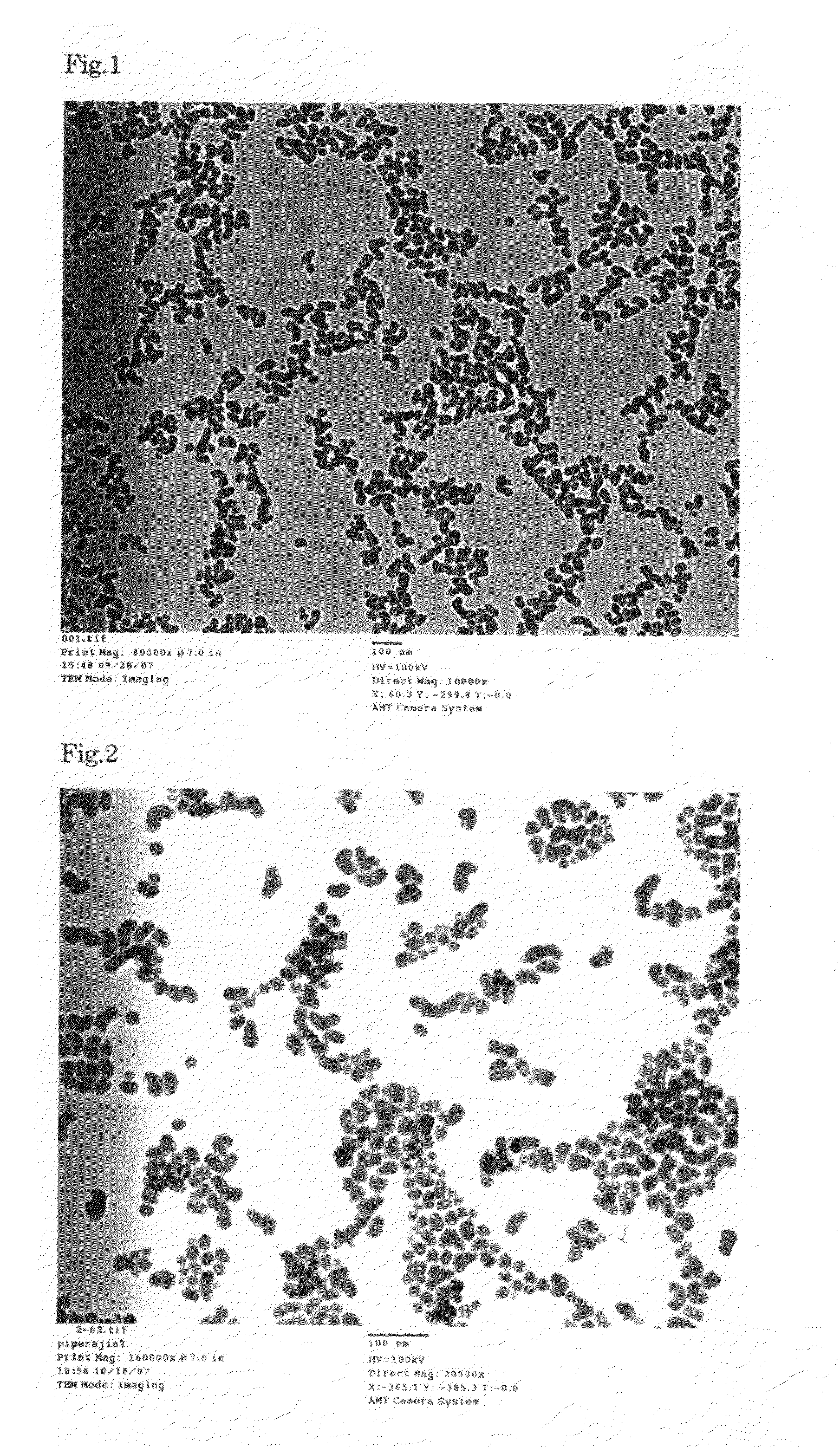
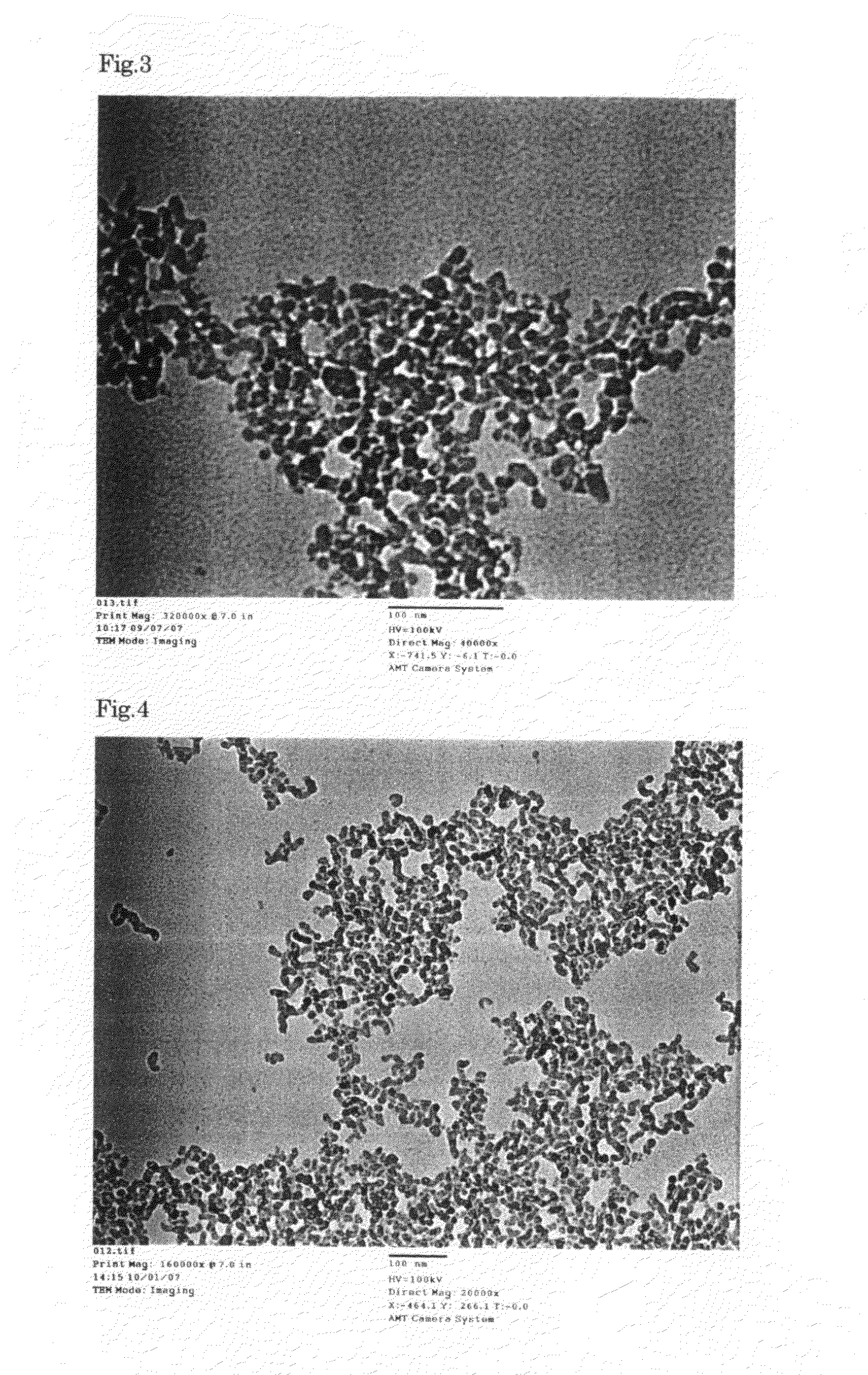
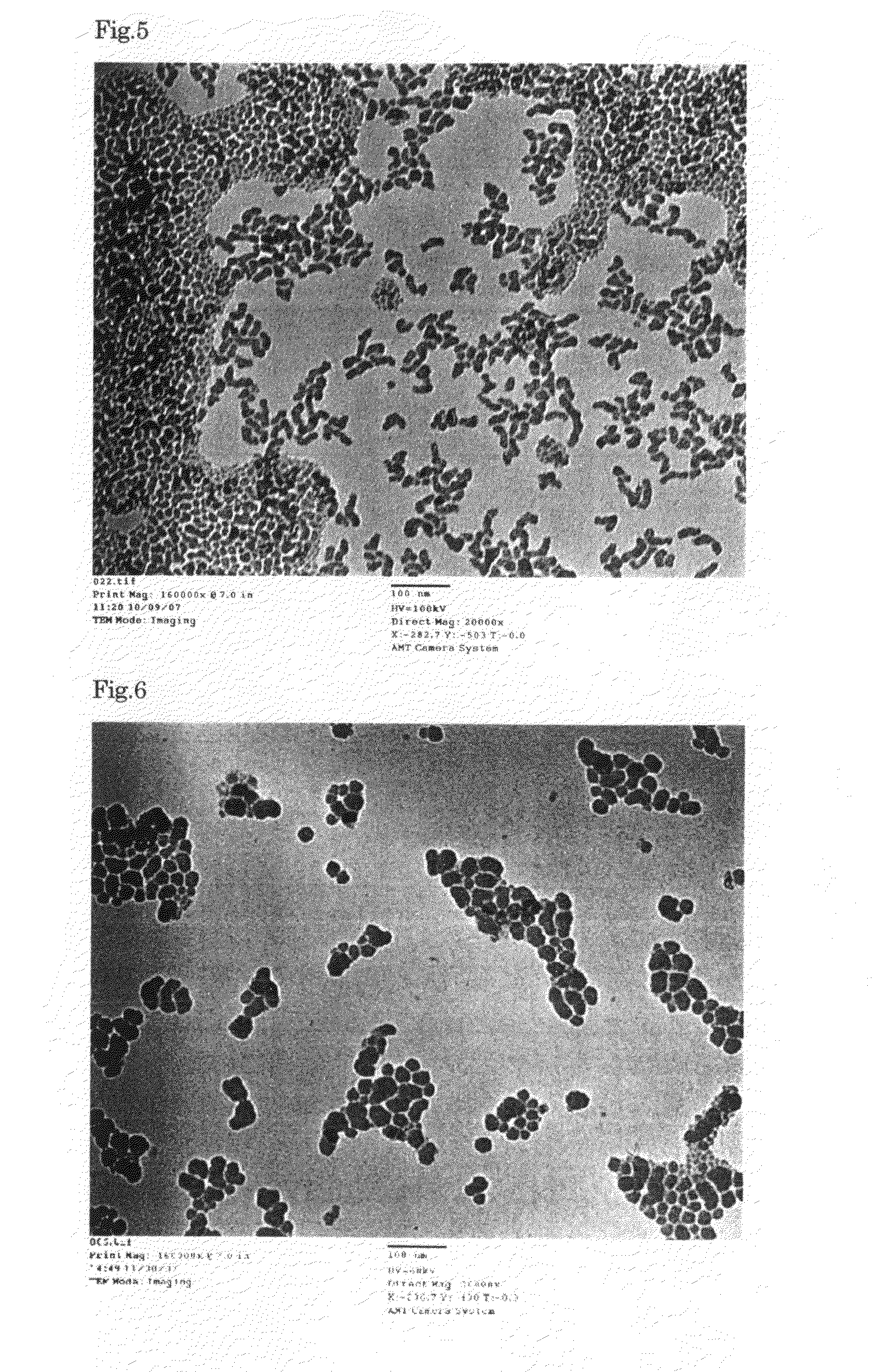
[0071]The present invention will be illustrated in more detail in Examples, although, these examples will not limit the previous invention. In Examples, following equipments are used for analysis of colloidal silica.

[0072](1) TEM observation: Transmission Electron Microscope H-7500 of Hitachi Ltd., is used.

[0073](2) Specific surface area by BET method: Flow Sorb 2300 of Shimadzu Corporation is used.

[0074](3) Analysis of nitrogen containing basic compounds except hydrazine: Total organic carbon meter TOC-5000A, SSM-5000A of Shimadzu Corporation is used. Carbon amount is converted into nitrogen containing basic compounds. Specifically, total organic carbon amount (TOC) is calculated by numerical formula of TOC=TC−IC after total carbon amount (TC) and inorganic carbon amount (IC) are measured. As a standard for TC measurement, a glucose aqueous solution of 1 weight % carbon amount is used, and as a standard for IC measurement, sodium carbonate of 1 weight % carbon amount is used. Ultra...

preparation example 1

[0078]5.2 kg of JIS 3 sodium silicate (SiO2: 28.8 weight %, Na2O: 9.7 weight %, H2O: 61.5 weight %) is added to 28 kg of deionized water, then mixed homogeneously and diluted sodium silicate having silica concentration of 4.5 weight % is prepared. This diluted sodium silicate is passed through a column containing 20 L of H type strong acidic cation exchange resin (AMBERLITE IR120B, product of ORGANO CORPORATION), which is previously regenerated by hydrochloric acid, and 40 kg of an active silicic acid aqueous solution having SiO2 concentration of 3.7 weight % and a pH of 2.9 is obtained. On the other hand, ethylenediamine anhydride (reagent) is added to deionized water and 10 weight % ethylenediamine aqueous solution is prepared.

[0079]Then, colloidal particles are grown up by a build up method. That is, 16 g of 10 weight % ethylenediamine aqueous solution is added to 500 g of said obtained active silicic acid aqueous solution while it is stirring and the pH is adjusted to 8.5. The s...

preparation example 2

[0081]By same method as Preparation Example 1, 40 kg of an active silicic acid aqueous solution having SiO2 concentration of 3.7 weight % and a pH of 2.9 is obtained. On the other hand, 34 g of crystal of diethylenediamine (piperazine, reagent) hexahydrate is dissolved in deionized water and total volume is brought to 190 g, to prepare 8 weight % aqueous solution.

[0082]30 g of 8 weight % diethylenediamine aqueous solution is added to 500 g of said obtained active silicic acid aqueous solution while it is stirring and the pH is adjusted to 8.5. The solution is heated to 100° C. and preserved 1 hour, then 9500 g of active silicic acid aqueous solution is added by 9 hours. During adding process, 8 weight % diethylenediamine aqueous solution is added so as to maintain the pH of 9 to 10 while heating (99° C.) is continued. Heating (99° C.) is continued 1 hour after adding process is over, then the solution is matured, and cooled down. In this process, 152 g of 8 weight % diethylenediamin...


PUM

PropertyMeasurementUnit
particle diameteraaaaaaaaaa
widthaaaaaaaaaa
widthaaaaaaaaaa

Abstract

A polishing composition for semiconductor wafer polishing comprising, colloidal silica prepared from an active silicic acid aqueous solution obtained by removal of alkali from alkali silicate and at least one nitrogen containing basic compound selected from a group consisting of ethylenediamine, diethylenediamine, imidazole, methylimidazole, piperidine, morpholine, arginine, and hydrazine, wherein pH of the colloidal silica is of 8.5 to 11.0 at 25° C. by containing quaternary ammonium hydroxide.

Description

FIELD OF THE INVENTION[0001]The present invention relates to polishing composition for semiconductor wafer that polishes a surface or an edge part of a semiconductor wafer such as a silicon wafer or a semiconductor device substrate with a film such as a metal film, an oxide film, a nitride film or the like (hereinafter shortened to metal films) on the surface.[0002]Hereinafter, “polishing composition for semiconductor wafer” can be shortened to “polishing composition”.BACKGROUND OF THE INVENTION[0003]Electronic components such as ICs, LSIs or ULSIs which applying semiconductor materials, such as silicon single crystal, as raw material can be manufactured based on a small semiconductor device chips. Said small semiconductor device chips are fabricated by dicing thin disk shaped wafers on which a number of fine electronic circuits are built to semiconductor chips, where the wafers are fabricated by slicing a single crystal ingot of silicon or semiconductors of other compound to thin d...

Claims


Application Information

Patent Timeline
Patent Type & Authority Applications(United States)
IPC IPC(8): C09K13/00B24B37/00C09K3/14H01L21/304
CPCC09G1/02C09K3/1463H01L21/02024
Inventor IZUMI, MASAHIRONAKAJO, MASARUSAITO, YUKIYOMAEJIMA, KUNIAKITANAKA, HIROAKI
Owner NIPPON CHECMICAL IND CO LTD
Why Eureka
Try Eureka