[0012]Thick doped or undoped nitride
layers on a
sapphire substrate have been developed using HVPE growth techniques. These layers range from 15 microns to over 150 microns in thickness. These thick nitride layers are optically smooth and exhibit less than 50 microns bow on a 2 inch
diameter sapphire wafer 430 microns thick at
room temperature. The bow limits enable higher yield during laser liftoff due to the finite
depth of field of the laser liftoff
system. These thick HVPE templates exhibit reduced
surface stress and higher
thermal conductivity than thinner templates, provide an epitaxial deposition ready surface, and are available in a variety of
dopant concentrations and profiles through the thickness of the nitride layers. The wafers exhibit no backside nitride growth, which enables complete separation of the nitride layer from the sapphire growth substrate without the use of backside
polishing. The GaN wafers exhibit an average alpha less than 1 cm−1 for all thicknesses and Si
doping levels less than 1019 for wavelengths greater than 395 nm. The formation of freestanding nitride templates with areas greater than 1 inch×1 inch have been demonstrated.
[0013]Templates based on nitride alloys of aluminum and
indium have been developed as well which enables the formation of templates that have their absorption properties either shifted to short wavelengths, as in the case of
aluminum gallium nitride (AlGaN) alloys, or longer wavelengths, based on
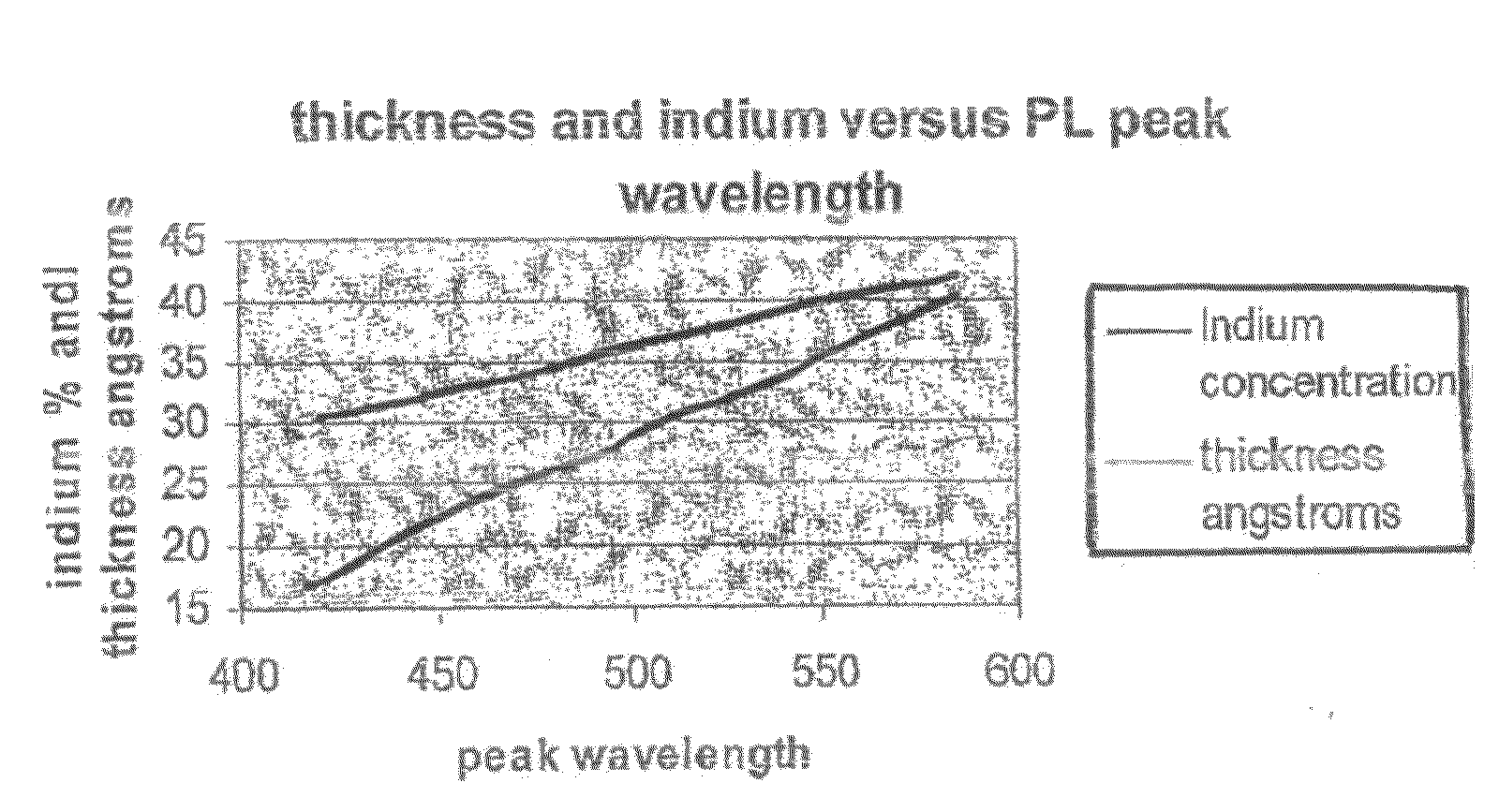
indium gallium nitride (InGaN) alloys. Aluminum
indium gallium nitride (AlInGaN) and other dilute nitrides can be used as templates. The nitride layers greater than 15 microns in thickness are
crack free. Upon separation, the nitride layers are flexible and can be bent or flattened. 30 micron thick nitride layers 1 inch×1 inch have been formed that are flexible and can be conformed to a variety of surfaces
ranging from flat to curve have a
radius greater than 1 cm. The lamination of these layers can form plywood like structures.
[0015]While alternate growth methods are possible and are embodiments of this invention, the focus will be on HVPE due to lower cost, lower average alpha, and higher
crystal quality compared to bulk, MOCVD, and MBE. The thick HYPE template can create higher quality nitride alloys compared to thinner templates. Even more preferred is the use of flexible freestanding all nitride templates based on laser liftoff of thick HVPE layers grown on sapphire growth substrates. In general, the use of thick HVPE templates creates higher efficiency LEDs due to the ability to create higher quality high indium concentration InGaN. The exact mechanisms, which lead to the improved InGaN growth, are unclear. While work from Berkeley on 5 and 15 micron MOCVD templates on sapphire indicates
enhanced growth rates on thicker templates (which they attribute to lower
surface stress in thick layers), their work was in the blue region of the spectrum and the MOCVD templates were cost prohibitive. Alternately, other authors have argued the opposite that increase stress within the wells increases indium incorporation. The present inventors have developed thick (greater than 15 microns) HYPE templates, which are cost effective, exhibit epitaxial deposition ready surfaces, reduced bow and low enough alpha to enable their use in this invention. Increased quality high indium InGaN can be grown on thick HYPE templates. Even more preferred is the use of flexible freestanding substantially all-nitride templates for increased quality high indium content InGaN.
[0016]A further
advantage of having a thick nitride layer is the ability to make surface modifications on a reasonable scale both within the device and on an external surface to the device. The use of subwavelength
surface modification is an embodiment but micron sized modifications or larger are preferred due to lower manufacturing costs. The removal of the thick nitride layer can create a freestanding device, both separately and in combination with the other disclosed inventions herein. These surface modifications can be on one side, both sides, and on edges of the templates.
Surface modification on both sides of at least one flexible freestanding substantially all-nitride foil is a preferred embodiment of this invention.
[0018]A thick HVPE template can be directly loaded into a MOCVD reactor, the MQWs only can be grown, the
wafer, tape, ribbon, foil, or
fiber form factor of the thick HYPE template can be removed from the MOCVD reactor and put into a MOCVD, MO-HVPE, or HVPE reactor and the AlGaN barrier and GaN p Layer can be grown successfully. While template growth has been demonstrated for complete structures, the growth of just the
quantum wells in one reactor followed by growth of the barrier and p layer in a separate reactor has not previously been demonstrated. Using this approach, the MQW MOCVD reactor can be tuned for optimum
quantum well growth, and the barrier and p layers can be done in a reactor tuned for efficient incorporation of Mg and Aluminum as required by those layers. In addition, it is an embodiment of this invention that the most preferred is the use of HVPE to form the barrier and p layers due to lower alpha, ability to increase aluminum concentration while maintaining
crystal quality, and ability to grow thicker higher crystal quality p type layers.
[0019]In addition, the use of multiple growth stages allows for the introduction of
surface modification between growth stages. This approach is applicable to nitrides, dilute nitrides, various alloys and other high bandgap materials such
a diamond. The use of these approaches are applicable to not only LEDs but laser diodes, power devices such as FET, HEMTs,
optoelectronics, MEMS, solar cells, and RF devices. Surface modifications may include, but are not limited, to
laser patterning, lithographic patterning (with the scale
ranging from 10 microns to a few angstroms), actinic
radiation modifications, implantation, diffusional
doping and combinations of these methods. The results of these methods include, but are not limited, to enhancing crystal quality, reducing
phonon reflections, creating light extraction, and creating an increased emission area. Similarly, these methods enable higher crystal quality growth and enhanced thermal performance devices for all semiconductor and electrical device applications. The ability to create these modifications is enabled by the thickness of the HVPE growth of the GaN semiconductor layer. It is most preferred that the thick nitride layer be greater than 15 microns and, even more preferred, that the thick nitride layer be greater than 30 microns. Surface modifications with feature depth to thick nitride
layer thickness ratios greater than 0.1 are most preferred. Controlled atmospheres between, during, or after these growth interruptions can create these surface modifications. The combination of improved crystal quality due to the thick nature of the HYPE template and surface modifications of the layer prior to any of the growth steps is an embodiment of this invention.
Surface modification can be on one or both sides of the HVPE template. A preferred embodiment is dual sided
processing of at least one flexible freestanding substantially all-nitride template.

