
Substantially Non-Oxidizing Plasma Treatment Devices and Processes

a plasma treatment device and plasma technology, applied in the field of substantial non-oxidizing plasma mediated processes and plasma treatment devices, can solve the problems of degrading transistor performance, increasing device leakage, and increasing leakage, and achieve the effect of inhibiting the formation of copper hydrid

Inactive Publication Date: 2011-06-09
LAM RES CORP
View PDF20 Cites 43 Cited by
  • Summary
  • Abstract
  • Description
  • Claims
  • Application Information

AI Technical Summary

Benefits of technology

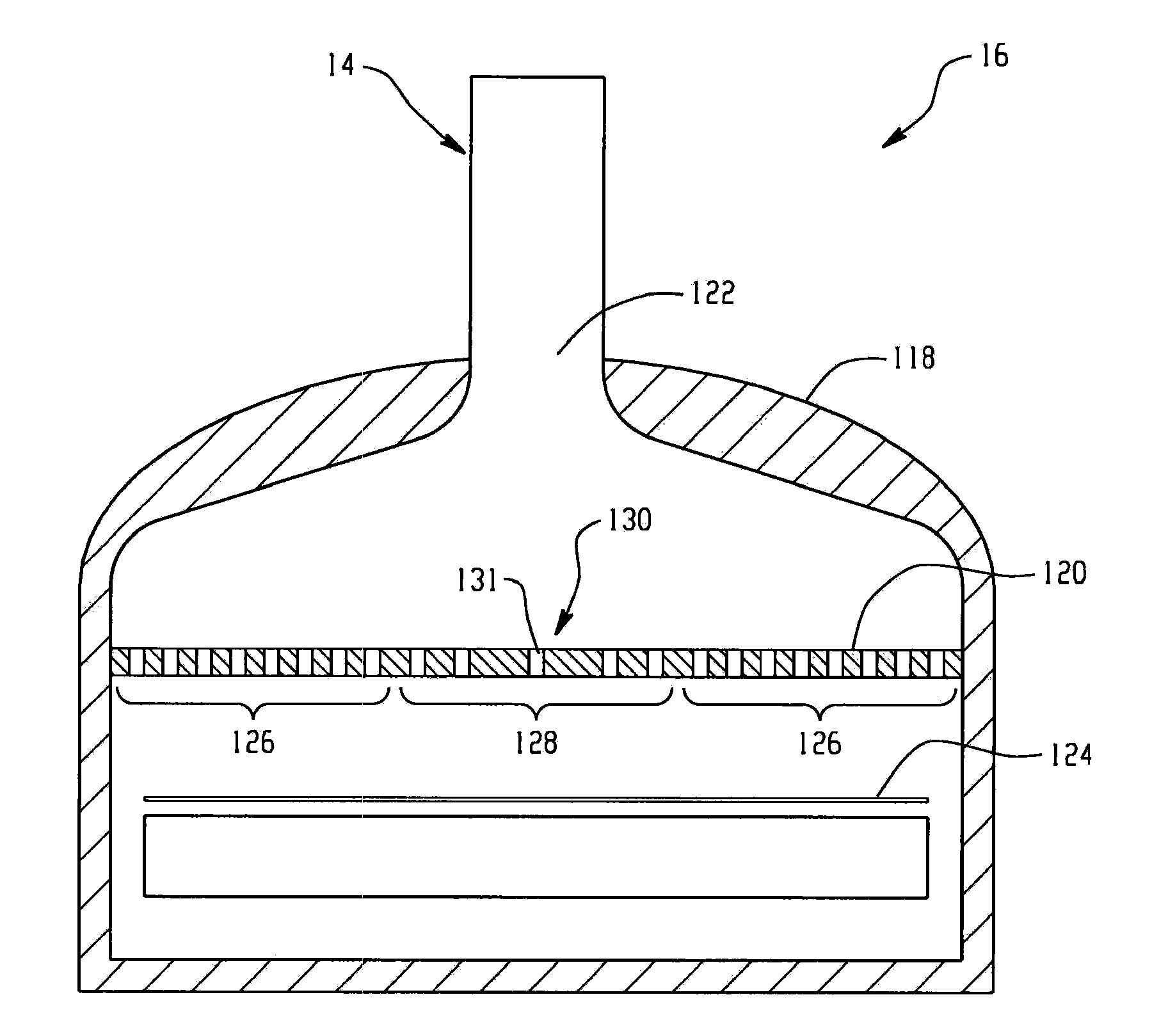
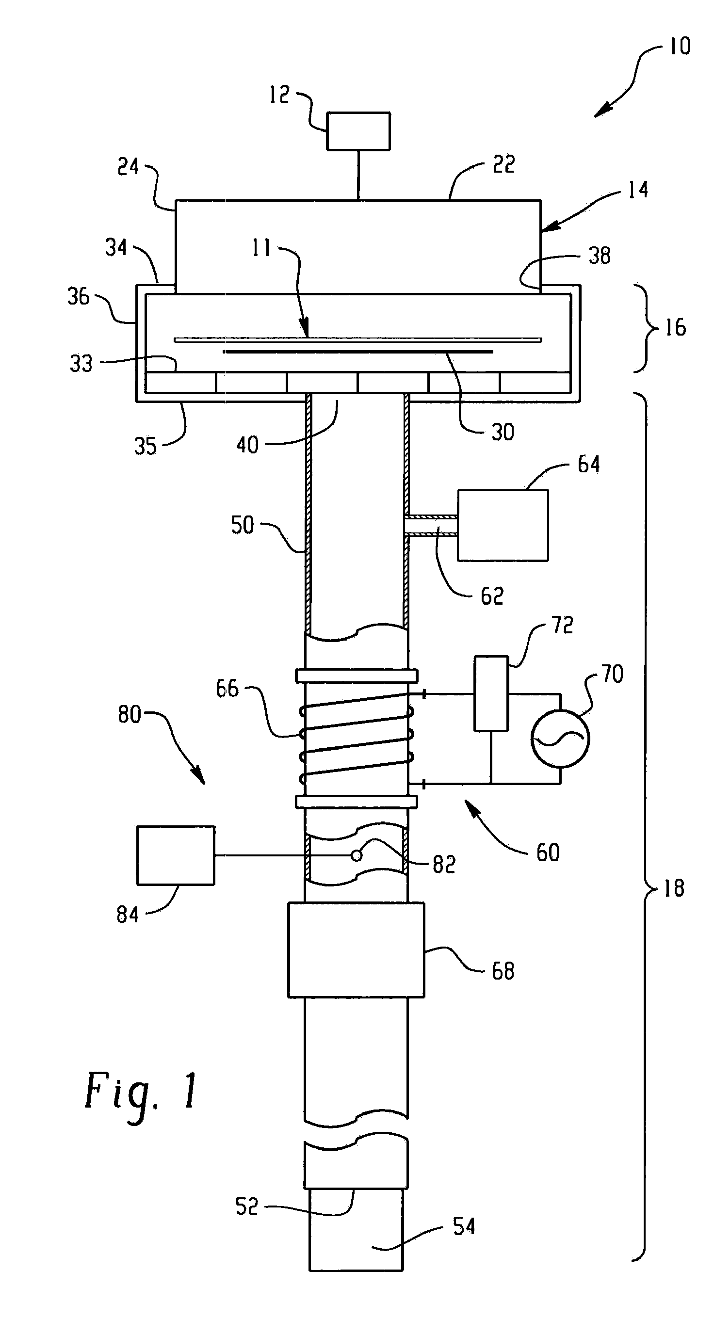
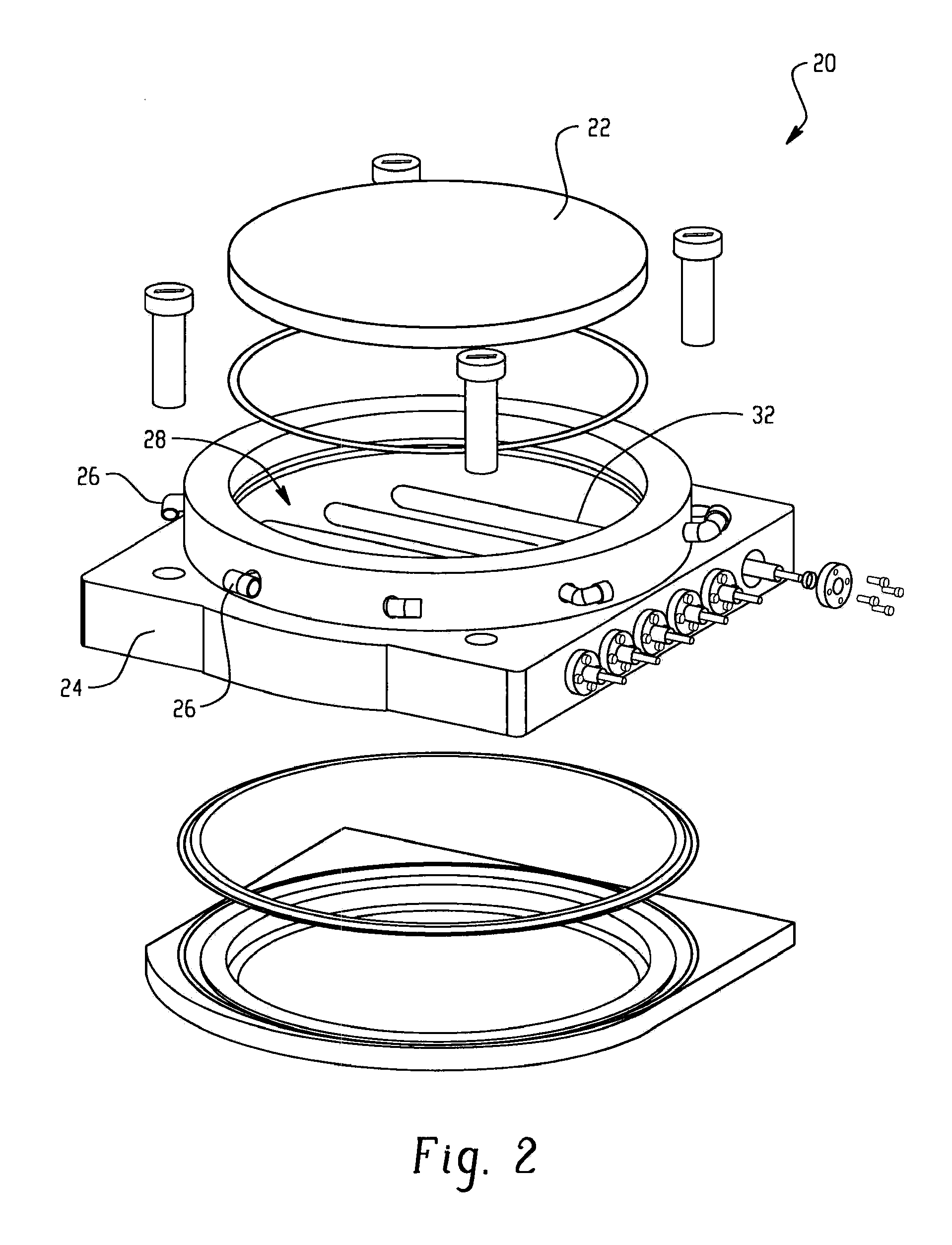
[0013]In still another embodiment, a plasma treatment device for treating a semiconductor workpiece comprises a gas inlet in fluid communication with a plasma generating component and configured to receive a substantially non-oxidizing gas source, wherein the plasma generating component is configured to generate plasma from the substantially non-oxidizing gas source during operation of the plasma treatment device; and a process chamber in fluid communication with the plasma generating component and configured to receive the plasma, wherein interior surfaces of the plasma treatment device are configured to be heated to a sufficient temperature to prevent photoresist and reaction byproduct buildup on the interior surfaces.
[0015]In another embodiment, a substantially non-oxidizing plasma process for removing photoresist from a substrate within a process chamber comprises exciting a gas mixture comprising a substantially non-oxidizing gas to form reactive plasma species wherein the substantially non-oxidizing gas comprises at least one gas selected from the group consisting of H2, NH3, N2H4, H2S, CH4, C2H6, C3H8, HF, H2O, HCl, HBr, HCN, CO, N2O, and combinations thereof; and selectively reacting photoresist on a semiconductor workpiece with the reactive plasma species to remove the photoresist from the substrate and form volatile photoresist and reaction byproducts, wherein surfaces exposed to the substantially non-oxidizing plasma contain a copper content sufficiently low to prevent copper contamination of the semiconductor workpiece to a level of less than or equal to 2×10¹⁰ copper atoms per cm2.

Problems solved by technology

As integrated devices become smaller, scaling of the gate dielectric causes increased leakage due to electron tunneling through the thin dielectric layer.
The ashing step is typically followed by a wet chemical treatment to remove traces of the ashing residue, which can cause device opens or shorts or lead to an increase in device leakage.
Additionally oxidizing plasma discharges can oxidize the silicon conduction channel under the high-k dielectric since most high-k dielectrics are poor diffusion barriers to the oxidizing plasma chemistry and the oxidizing plasmas can change the oxygen content or oxidation state of the high-k dielectric itself.
All cases result in degraded transistor performance.
The buildup of these ashing materials can lead to short mean-time-between-clean (MTBC) times and frequent rebuild / replacement of vacuum hardware resulting in loss of throughput and increased costs of ownership.
Additionally, deposits of the fragmented photoresist material and ashing byproducts within the process chamber that are located above the plane of the substrate can lead to particulate contamination on the substrate, thereby further affecting device yields.
An additional problem with non-oxidizing plasma discharges, such as the hydrogen and nitrogen based plasma discussed above, is the non-uniformity of the plasma exposure especially for prior art apparatuses that have been optimized for oxidizing plasmas.
It has been found that the less aggressive substantially non-oxidizing plasma discharges have fewer reactive species and the dispersal from the center point of the baffle plate to its outer edge can result in hot spots on the wafer, i.e., areas of non-uniformity.
Still further, it has been discovered that many oxides and ceramics degrade and / or devitrify under exposure to substantially non-oxidizing plasmas at elevated temperatures.
This degradation / devitrification can lead to particle formation and ultimately failure of the component.

Method used


Image

  • Substantially Non-Oxidizing Plasma Treatment Devices and Processes
  • Substantially Non-Oxidizing Plasma Treatment Devices and Processes
  • Substantially Non-Oxidizing Plasma Treatment Devices and Processes

Examples


example 1

[0068]In this example, bare silicon wafers were exposed to plasma generated from forming gas in a RapidStrip320 plasma ashing tool commercially available from Axcelis Technologies, Inc., Beverly, Mass. Different processing chamber configurations of different materials were employed. Copper metal contamination levels of the bare silicon wafers was determined after plasma processing by vapor phase decomposition with inductively coupled plasma mass spectrometer analysis (VDP ICP-MS). The plasma chemistry was formed by flowing forming gas (5% Hydrogen in Nitrogen) at 7 standard liters per minute (slm) into the plasma ashing tool at a pressure of 1 Torr, a wafer temperature of 275° C., and a power setting of 3500 Watts.

[0069]FIG. 8 graphically illustrates the results for both the absolute copper amount (atms / cm2) and the relative copper amount (detected copper atoms / total atoms of 11 probed metals in %). The process chamber configured with a chuck formed of an aluminum alloy demonstrated...

example 2

[0070]In this example, a substrate having a TiN coating deposited thereon was exposed to plasmas formed from a gas mixture containing varying amounts of oxygen and NH3 and a gas mixture that contained varying amounts of oxygen and a 5% by volume hydrogen gas / helium gas mixture without any nitrogen present in the mixture. The results are shown in FIGS. 9 and 10.

[0071]FIG. 9 graphically illustrates the amount of oxidation of a TiN material exposed to a plasma gas mixture of NH3 and O2 for 3 minutes, with chuck temperature at 240° C. For O2 concentrations of <about 25%, the results showed that TiN oxidation is ≦0.1 nm for the exposure conditions. Thus, these results demonstrate the plasma was substantially non-oxidizing when the TiN material was exposed to plasma generated from a gas mixture containing less than 25% by volume.

[0072]FIG. 10 graphically illustrates the amount of TiN loss as a result of oxidation as a function of the amount of oxygen contained in the mixture of O2 and the...


PUM

PropertyMeasurementUnit
Temperatureaaaaaaaaaa

Abstract

Non-oxidizing plasma treatment devices for treating a semiconductor workpiece generally include a substantially non-oxidizing gas source; a plasma generating component in fluid communication with the non-oxidizing gas source; a process chamber in fluid communication with the plasma generating component, and an exhaust conduit centrally located in a bottom wall of the process chamber. In one embodiment, the process chamber is formed of an aluminum alloy containing less than 0.15% copper by weight; In other embodiments, the process chamber includes a coating of a non-copper containing material to prevent formation of copper hydride during processing with substantially non-oxidizing plasma. In still other embodiments, the process chamber walls are configured to be heated during plasma processing. Also disclosed are non-oxidizing plasma processes.

Description

BACKGROUND[0001]The present disclosure relates to semiconductor apparatuses and processes, and more particularly, to substantially non-oxidizing plasma mediated processes and plasma treatment devices suitable for treating a semiconductor workpiece.[0002]Recently, much attention has been focused on developing high-k dielectrics with metal gates to enable scaling of devices. As integrated devices become smaller, scaling of the gate dielectric causes increased leakage due to electron tunneling through the thin dielectric layer. A solution to this problem is to implement a gate dielectric with higher dielectric constant (also referred to as “high k”). As used herein, the term “high k” generally refers to a dielectric constant greater than silicon dioxide. The use of high k dielectric layers as gate insulator layers allow thicker layers to be used, with the thicker high k dielectric layer supplying capacitances equal to thinner silicon oxide layers, or with the high k dielectric layer ha...

Claims


Application Information

Patent Timeline
IPC IPC(8): H01L21/3065G03F7/42B08B7/00
CPCH01J37/32357H01J37/32477H01J37/32504H01L21/67069H01J37/32935H01L21/31138Y02C20/30H01J37/32844Y02P70/50
Inventor GEISSBUHLER, PHILLIPBERRY, IVANHUSEINOVIC, ARMINLUO, SHIJIANSRIVASTAVA, ASEEM KUMARWALDFRIED, CARLO
Owner LAM RES CORP
Learn More