Photocurable and thermally curable thiosulfate-containing polymers

a technology of thiosulfate and polymer, which is applied in the field of unique photocurable and thermally curable thiosulfate-containing polymers, can solve the problems of amorphous silicon, limited application of amorphous silicon to low speed devices, and amorphous silicon still has its drawbacks, so as to improve the properties of organic film-forming polymeric precursor dielectric materials, improve the effect of organic field effect transistors and easy manufacturing

Active Publication Date: 2016-09-27
EASTMAN KODAK CO
View PDF16 Cites 3 Cited by
  • Summary
  • Abstract
  • Description
  • Claims
  • Application Information

AI Technical Summary

Benefits of technology

[0045]The present invention provides photocurable or thermally curable thiosulfate-containing polymers for precursor dielectric compositions (usually in the form of layers), and associated semiconductor devices that address various deficiencies and shortcomings in organic polymers used as dielectric layers in the art. The present invention provides materials for improving the properties of organic field effect transistors (OFET's) including n-type or p-type organic field effect thin film transistors, using improved organic film-forming polymeric precursor dielectric materials. The resulting devices of this invention can be readily manufactured using low-cost processes.

Problems solved by technology
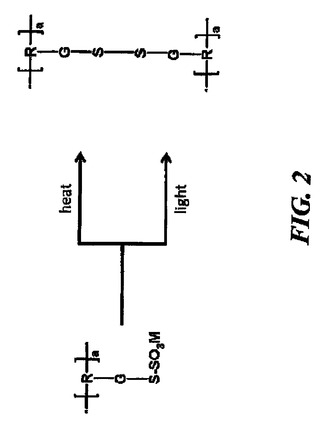
Application of amorphous silicon is limited to low speed devices, however, since its maximum mobility (0.5-1.0 cm2 / V·sec) is about a thousand times smaller than that of crystalline silicon.
Although amorphous silicon is less expensive than highly crystalline silicon for use in TFT's, amorphous silicon still has its drawbacks.
The deposition of amorphous silicon, during the manufacture of transistors, requires relatively costly processes, such as plasma enhanced chemical vapor deposition and high temperatures (about 360° C.) to achieve the electrical characteristics sufficient for display applications.
Such high processing temperatures disallow the use of substrates, for deposition, made of certain plastics that might otherwise be desirable for use in applications such as flexible displays.
Lower processing temperatures usually lead to poor quality films with pinholes, resulting in poor insulating properties.
As a result it is necessary to use thick layers (more than 100 nm) to ensure sufficiently good insulator properties which results in increased supply voltages for operation of such circuits.
Another widely used process is ion beam deposition, but it needs high vacuum and expensive equipment that are incompatible with the goal of very low cost production.
Similarly, use of other high dielectric constant inorganic materials as barium zirconate titanate (BZT) and barium strontium titanate (BST) need either a high firing temperature (400° C.) for the sol-gel process, or radiofrequency magnetron sputtering, which also requires vacuum equipment, and can also have stoichiometric problems.
It has been shown that the presence of polar functionalities (like —OH groups on SiO2 surface) at the dielectric-organic semiconductor interface trap charges which results in lowers carrier mobility in organic semiconductors.
This results in a low energy dielectric surface with very few chemical defects or reactive functionalities that could adversely affect the OFET device performance.
Most organic materials used in OFET's cannot withstand the high processing temperatures used with conventional inorganic materials.
For example, the 200° C. or higher temperatures needed to process conventional inorganic materials would at the very least cause a polymeric substrate to deform, and might cause further breakdown of the polymer or even ignition at high enough temperatures.
Deformation is highly undesirable, since each layer of the structure has to be carefully registered with the layers below it, which becomes difficult to impossible when the layers below it are deformed due to processing temperatures.
Polymers generally have the advantage that they can be processed at relatively low temperatures below 200° C. However, compared to inorganic dielectrics, the insulating property of thin layers of polymeric dielectrics is usually poor on account of leakage currents.
However, this attempt is limited in usefulness since a high temperature of about 200° C. is required to attain crosslinking.
However, the presence of acid is not desirable since it could have deleterious effect on the performance of OFET's.
However, the presence of polar groups at the dielectric interface creates dipolar disorder that lowers the carrier mobility.
However, the presence of hydroxyl groups at the organic semiconductor gate dielectric interface is not desirable as hydroxyl trap charges.
Although OFET device performance may improve in the presence of fluorine containing polymer, the process requires undesirably coating multiple polymer layers.
While a number of dielectric compositions and materials have been proposed for uses in OFET devices, polymer dielectric materials that work well in p-type or p-channel OFET's usually do not necessarily perform as well with OFET's comprising n-type semiconductors.
Although various polymer dielectric compositions are known, a number of problems still remain in terms of the process of making such dielectric layers and improving overall performance in OFET's.
As discussed before, some the polymer dielectric compositions require coating of multiple layers that is a difficult and costly process.
It is difficult to crosslink all phenolic groups during thermal annealing and thus the presence of phenolic groups in dielectric is not desirable.
Furthermore, most polymer materials are usually not appropriate for use in low voltage applications due to their low dielectric constant (k).
However, when this method is used, the thickness of the insulating film is limited to the size of the inorganic material thus ground.
Furthermore, since a solid material is dispersed in an organic polymer solution, an uneven dispersion is formed, possibly causing the generation of local electric field and concurrent dielectric breakdown during the operation of transistor.
Importantly, since the inorganic material is merely present in the organic polymer and thus does not compensate the chemical resistance of the insulating film, the resulting insulating film cannot be subjected to any processes involving the use of solvents.
However, the thin ceramic film is an insulating film made of an inorganic material that can be applied to silicon wafer, which is nonflexible and hard, but it cannot be applied to flexible substrates.
However, pentacene based OFET having an azole-metal complex compound as a dielectric shows lower mobility and poor current on / off ratio.
However, surface roughness of such films is quite high (about 2.1 nm).
Although various polymer dielectric compositions are known, a number of problems still remain in terms of the process of making such dielectric layers and improving overall performance in OFET's.
However, these methods do not result in crosslinking of the dielectric layer, which is a key requirement in solution processable OFET's.
Since most of the polymer dielectrics known in prior art are not crosslinked, the resulting dielectric film cannot be subjected to any processes involving the use of solvents.
However, this approach has limited application since a high temperature of about 200° C. is required to attain crosslinking.
It is difficult to find polymeric materials that have all of these properties because some polymers will exhibit improvements in some of the properties but exhibit worse effects in others.

Method used


Image

  • Photocurable and thermally curable thiosulfate-containing polymers
  • Photocurable and thermally curable thiosulfate-containing polymers
  • Photocurable and thermally curable thiosulfate-containing polymers

Examples


##ventive example 1

Inventive Example 1

Preparation of Poly(vinyl benzyl thiosulfate sodium salt-co-methyl methacrylate-co-N-butyl-N′-[2-(ethoxy-2-acrylate)ethyl]-1,4,5,8-naphthalenetetracarboxylic diimide)

[0224]The procedure of Synthesis 1 was followed using vinyl benzyl chloride (4.2 g, 0.027 mol), methyl methacrylate (8.5 g, 0.085 mol), 1,8-naphthalimidohexanol (1.1 g, 0.002 mol), 2,2′-azobis(2-methylbutyronitrile) (0.33 g, 0.002 mol), and 47 ml of toluene. The reaction temperature was 70° C. 1H NMR analysis indicated that the resulting precursor polymer contained 30 mol % of recurring units derived from vinyl benzyl chloride. Analysis by size exclusion chromatography (SEC) indicated a weight average molar mass of 17,800 (polystyrene standards).

[0225]The desired photocurable or thermally curable thiosulfate-containing polymer was prepared as described in Synthesis 1 using 1.35 g of the precursor polymer, 50 ml of DMF, 1.5 g of sodium thiosulfate, and 10 ml of water. The temperature of the reaction so...

##ventive example 2

Inventive Example 2

Preparation of Poly(vinyl benzyl thiosulfate sodium salt-co-methyl methacrylate-co-acrylic acid-co-N-butyl-N′-[2-(ethoxy-2-acrylate)ethyl]-1,4,5,8-naphthalenetetracarboxylic diimide)

[0226]The procedure of Synthesis 1 was followed using vinyl benzyl chloride (8.2 g, 0.053 mol), methyl methacrylate (8.5 g, 0.085 mol), acrylic acid (8.5 g, 0.119 mol), 1,8-naphthalimidohexanol (2.3 g, 0.005 mol), 2,2′-azobis(2-methylbutyronitrile) (0.76 g, 0.004 mol), and 90 ml of dioxane. The reaction temperature was 70° C. 1H NMR analysis indicated that the resulting precursor polymer contained 30 mol % of recurring units derived from vinyl benzyl chloride. Analysis by size exclusion chromatography (SEC) indicated a weight average molar mass of 41,600 (polystyrene standards).

[0227]The desired photocurable or thermally-curable thiosulfate-containing polymer was prepared as described in Synthesis 1 using 26.1 g of the precursor polymer, 285 ml of DMF, 8.5 g sodium thiosulfate, and 57 ...

##ventive example 3

Inventive Example 3

Preparation of Poly(vinyl benzyl thiosulfate sodium salt-co-acrylic acid-co-N-butyl-N′-[2-(ethoxy-2-acrylate)ethyl]-1,4,5,8-naphthalenetetracarboxylic diimide)

[0228]The procedure of Synthesis 1 was followed using vinyl benzyl chloride (7.3 g, 0.048 mol), acrylic acid (15.0 g, 0.21 mol), 1,8-naphthalimidohexanol (1.9 g, 0.005 mol), 2,2′-azobis(2-methylbutyronitrile) (0.76 g, 0.004 mol), and 73 ml of dioxane. The reaction temperature was 70° C. 1H NMR analysis indicated that the resulting precursor polymer contained 31 mol % of recurring units derived from vinyl benzyl chloride. Analysis by size exclusion chromatography (SEC) indicated a weight average molar mass of 21,400 (polystyrene standards).

[0229]The desired photocurable or thermally-curable thiosulfate-containing polymer was prepared as described in Synthesis 1 using 20.0 g of the precursor polymer, 250 ml of DMF, 6.5 g sodium thiosulfate, and 50 ml of water. The reaction temperature was 90° C. for 8 hours to...


PUM

PropertyMeasurementUnit
Tgaaaaaaaaaa
temperaturesaaaaaaaaaa
temperatureaaaaaaaaaa

Abstract

Photocurable or thermally curable thiosulfate-containing polymers have a Tg of at least 50° C. and (a) recurring units comprising pendant thiosulfate groups, and (b) recurring units comprising organic charge balancing cations that are associated with the (a) recurring units sufficiently to provide a net neutral charge with the pendant thiosulfate groups. These polymers can be represented by the following Structure (III):wherein R represents the organic polymer backbone, G is a single bond or a divalent linking group, M+ represents the organic charge balancing cation, and “a” represents at least 0.5 mol % and up to and including 50 mol % of (a) recurring units, and “b” represents the (b) recurring units and is at least equal to the “a” mol %, based on the total recurring units. These thiosulfate-containing polymers can be used to made dielectric compositions and gate dielectric layers in various devices.

Description

RELATED APPLICATIONS[0001]Reference is made to the following copending and commonly assigned patent applications, the disclosures of which are incorporated herein by reference:[0002]U.S. Ser. No. 14 / 301,370 (filed on Jun. 11, 2014, by Shukla and Donovan, published as U.S. 2015 / 0364687), and entitled “Devices Having Dielectric Layers with Thiosulfate-containing Polymers;”[0003]U.S. Ser. No. 14 / 301,380 (filed on Jun. 11, 2014, by Shukla, Mis, and Donovan, published as U.S. 2015 / 0361206), and entitled “Thiosulfate-containing Polymers Associated with Photosensitizer Component;” and[0004]U.S. Ser. No. 14 / 301,385 (filed on Jun. 11, 2014, by Shukla, Donovan, and Mis, published as U.S. 2015 / 0364688), and entitled Precursor Dielectric Composition with Thiosulfate-Containing Polymers.FIELD OF THE INVENTION[0005]This invention relates to unique photocurable and thermally curable thiosulfate-containing polymers that can be used to provide various devices such as organic field effect transistors...

Claims


Application Information

Patent Timeline
Patent Type & Authority Patents(United States)
IPC IPC(8): C08F222/10H01L51/00H01L51/05C08F220/10C08L81/08
CPCC08F220/10H01L51/0035H01L51/052C08F220/14C08F212/26C08F212/30H10K10/471H10K10/466H10K10/464C08F212/14C08F220/303C08F220/36C08F220/1808H10K85/111
Inventor SHUKLA, DEEPAKDONOVAN, KEVIN M.
Owner EASTMAN KODAK CO
Why Eureka
Try Eureka