
Substrate for thin film formation, thin film substrate, and light-emitting device

a technology of thin film substrate and substrate, applied in the direction of chemically reactive gases, electrical devices, crystal growth process, etc., to achieve the effect of comparatively easy manufacturing and relatively easy manufacturing

Inactive Publication Date: 2006-07-27
MIYAHARA KENICHIRO
View PDF9 Cites 82 Cited by
  • Summary
  • Abstract
  • Description
  • Claims
  • Application Information

AI Technical Summary

Benefits of technology

[0045] Using the above thin film substrate, it became clear that an optical waveguide in which the transmission loss is small and which can transmit ultraviolet light in low loss can be manufactured.
[0079] A boron component can be contained in the above thin film comprising as a main component at least one selected from gallium nitride, indium nitride and aluminum nitride and contains a single crystal or a single crystal layer at least, it was found that it is unified more firmly with the ceramic-based sintered compact. It was also found that the light-emitting device which emits the light of short wavelength 200 or less nm by using the thin film containing such a boron component can produce.

Problems solved by technology

When it is going to use a light-emitting device for such an intended use, as for the substrate for forming a thin film comprising an epitaxial film as the main substance and comprising as a main component at least one selected from gallium nitride, indium nitride and aluminum nitride and constitutes a light-emitting device, problems are arising.
However, since it is easy to generate a crystal dislocation and a strain in the thin film by the crystal lattice mismatching or difference of thermal expansion coefficient between the sapphire substrate and the thin film, even if it is a single-crystal thin film with high crystallinity, manufacture yield of the light-emitting device manufactured using such a thin film tends to be lowered, and achievement of the improvement in luminous efficiency of a light-emitting device or improvement in characteristics, such as high-output-izing and long-life of a laser oscillation, is also difficult.
Since a sapphire substrate is a single crystal, manufacture cost is also highly, and there is a problem in which it can be hard to use for an extensive use the single-crystal thin film comprising as a main component at least one selected from gallium nitride, indium nitride and aluminum nitride and formed on it.
In conventional optical waveguides, there are problems that they have low permeability to short-wavelength light such as blue or ultraviolet rays, that it is hard to form electrical circuits simultaneously on the substrate in which an optical waveguide is formed because the electric insulation of a substrate is small, and that it is hard to mount simultaneously a high-output light-emitting device on the substrate in which an optical waveguide is formed because the thermal conductivity of a substrate is low, etc.
However, when using a sapphire substrate, the luminous efficiency of the light-emitting device constituted mainly with such a thin film is low and is usually about 2-8%, so 92-98% of the electric power applied to the device is consumed other than the radiant power output to the outside of a device, and the light emitting characteristics in which the III-V group nitride semiconductor originally has have not been shown sufficiently.
As the cause, it is easy to produce a crystal dislocation and a distortion in the thin film by the crystal lattice mismatching, or the difference of thermal expansion coefficient between the sapphire substrate and the thin film, even if the thin film constituting a light-emitting device can be formed on a sapphire substrate as a single-crystal thin film with high crystallinity, furthermore, it seems that many of light emitted from the light-emitting device are reflected in the interface of the sapphire substrate and the above thin film, or in the surface of a sapphire substrate, and are easily shut up by being returned into the inside of a light-emitting device because the refractive index of a sapphire substrate is still smaller than a thin film of gallium nitride, indium nitride, and aluminum nitride, a sapphire substrate is a transparent and homogeneous bulk single crystal.
However, even if these substrates are used, a good single-crystal thin film is hard to be formed on these substrates for the reasons of the difference of a crystal structure and a lattice constant between the substrates and the single-crystal thin film comprising as a main component at least one selected from gallium nitride, indium nitride and aluminum nitride.
However, although this method must form the film material comprising an oxide of II group elements, such as zinc oxide and mercury oxide, before forming gallium nitride system compound semiconductor layer on a substrate, that effect is not necessarily clarified.
The thin film substrate having the above excellent single-crystal thin film comprising as a main component at least one selected from gallium nitride, indium nitride and aluminum nitride, however, has not be provided yet.
Thus, the luminous efficiency of the light-emitting device which is made using a conventional sapphire substrate is low, so it is hard to say that the original luminescence characteristics of III-V group nitride semiconductor can be shown sufficiently, though that having at least equivalent luminous efficiency to the light emitting device produced using a sapphire substrate is requested, the luminous efficiency of the light-emitting device produced using substrates proposed to improve the fault of a sapphire substrate instead of a sapphire substrate has not improved, and there was a problem in which the original luminescence characteristics of III-V group nitride semiconductor have not realized yet sufficiently.
As the reason of such a device, because there is a mismatching of crystal lattice, or a difference of thermal expansion coefficient between the silicon and sapphire of the substrate material and the aluminum nitride, it is probably surmised that it will be because formation of an aluminum nitride thin film with high crystallinity is difficult, and transmission loss of a waveguide becomes large as a result.
Other than the mismatching of crystal lattice, and the difference of thermal expansion coefficient, when the silicon substrate is used, it seems a big cause that it does not function as a waveguide too, since a total reflection of light does not occur in the aluminum nitride thin film because the refractive index of an aluminum nitride thin film formed directly is small if it is compared with the silicon.
Since the electric insulation nature is small and the dielectric constant is high when silicon is used for a substrate, it can be hard to form an electrical circuit on a substrate directly, and there is a problem in which it can be hard to mount a light-emitting device on the substrate unitedly.
When using the sapphire for a substrate, in case a high-output light-emitting device is mounted, a problem of the nature of radiating heat arises since the thermal conductivity is small.
Therefore, there were problems, such that the satisfactory optical waveguide which transmits a light with short wavelength, such as blue light and ultraviolet rays, from a light-emitting device provided with an electric circuit for driving a device and can mount a high power light-emitting device has not been realized.

Method used


Image

  • Substrate for thin film formation, thin film substrate, and light-emitting device
  • Substrate for thin film formation, thin film substrate, and light-emitting device
  • Substrate for thin film formation, thin film substrate, and light-emitting device

Examples


example 1

[0751] High-purity, submicron ceramic raw material powders used were aluminum nitride powder of grade “F” available from Tokuyama, Inc., silicon carbide powder of grade “OY-15” available from Yakushima Denko Co., Ltd., silicon nitride powder of grade “SN-E05” available from Ube Industries, Ltd., aluminum oxide powder of grade “AKP-30” available from Sumitomo Chemical Co., Ltd., partially stabilized zirconia powder of grade “TZ-3Y” containing 3 mol % of Y2O3 as a stabilization agent available from TOSOH CORP., zinc oxide of “first grade” available from Sakai Chemical Industry Co., Ltd., guaranteed magnesium oxide powder available from Kanto Kagaku, and beryllium oide powder and magnesium aluminate (MgAl2O4: spinel) powder both available from Kojundo Chemical Laboratory Co., Ltd. The purity was not less than 99 weight % except for partially stabilized zirconia. The oxygen content was 1.0 weight % in the aluminum nitride powder. 1.0% by weight of B4C powder and 1.0% by weight of carbon...

example 2

[0788] As for the crystallinity of the single-crystal thin film comprising as a main component at least one selected from gallium nitride, indium nitride and aluminum nitride and is formed directly on the aluminum nitride-based sintered compact substrate, the influence by the characteristics, such as the composition of the aluminum nitride-based sintered compact, the microstructure of the sintered compact, and the optical transmissivity, etc., was investigated.

[0789] As the raw material powder for sintered compact production used for the experiment the same high purity aluminum nitride powder [the grade “F” by Tokuyama Soda Co., Ltd. (present: Tokuyama, Inc.)] as those having been used in Example 1 was prepared.

[0790] The raw material powder is manufactured by the method of oxide reduction.

[0791] After additives, such as sintering aids, and blackening agents, etc., are suitably added to the raw material powder, it mixes by the ball mill with ethanol for 24 hours, and it was dried...

example 3

[0809] High purity aluminum nitride powder (the grade “H” available from Tokuyama, Inc.) was prepared as the raw material powder for producing an aluminum nitride-based sintered compact. This raw material powder was manufactured by the method of oxide reductionin. This raw material powder contains oxygen 1.3 weight % as impurities.

[0810] Added to this raw material powder were 3.3 volume % of Y2O3 powder, 4.02 volume % of Er2O3 powder, and 0.6 volume % by of CaCO3 powder on a CaO basis, and mixed with toluene and isopropyl alcohol by the ball mill for 24 hours, then an acrylic binder was added 12 weight parts to 100 weight parts of the powder raw materials, furthermore they were mixed for 12 hours and made into a paste, and the green sheets having three kinds of composition as thick as 0.75 mm by the doctor blade method were produced.

[0811] The green sheets were formed into square sheets of 35 mm×35 mm, to which circular through-holes having a diameter of 25 μm, 50 μm, 250 μm and 5...


PUM

PropertyMeasurementUnit
temperatureaaaaaaaaaa
sizeaaaaaaaaaa
particle diameteraaaaaaaaaa

Abstract

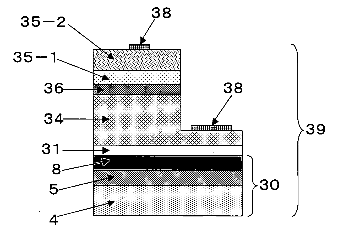
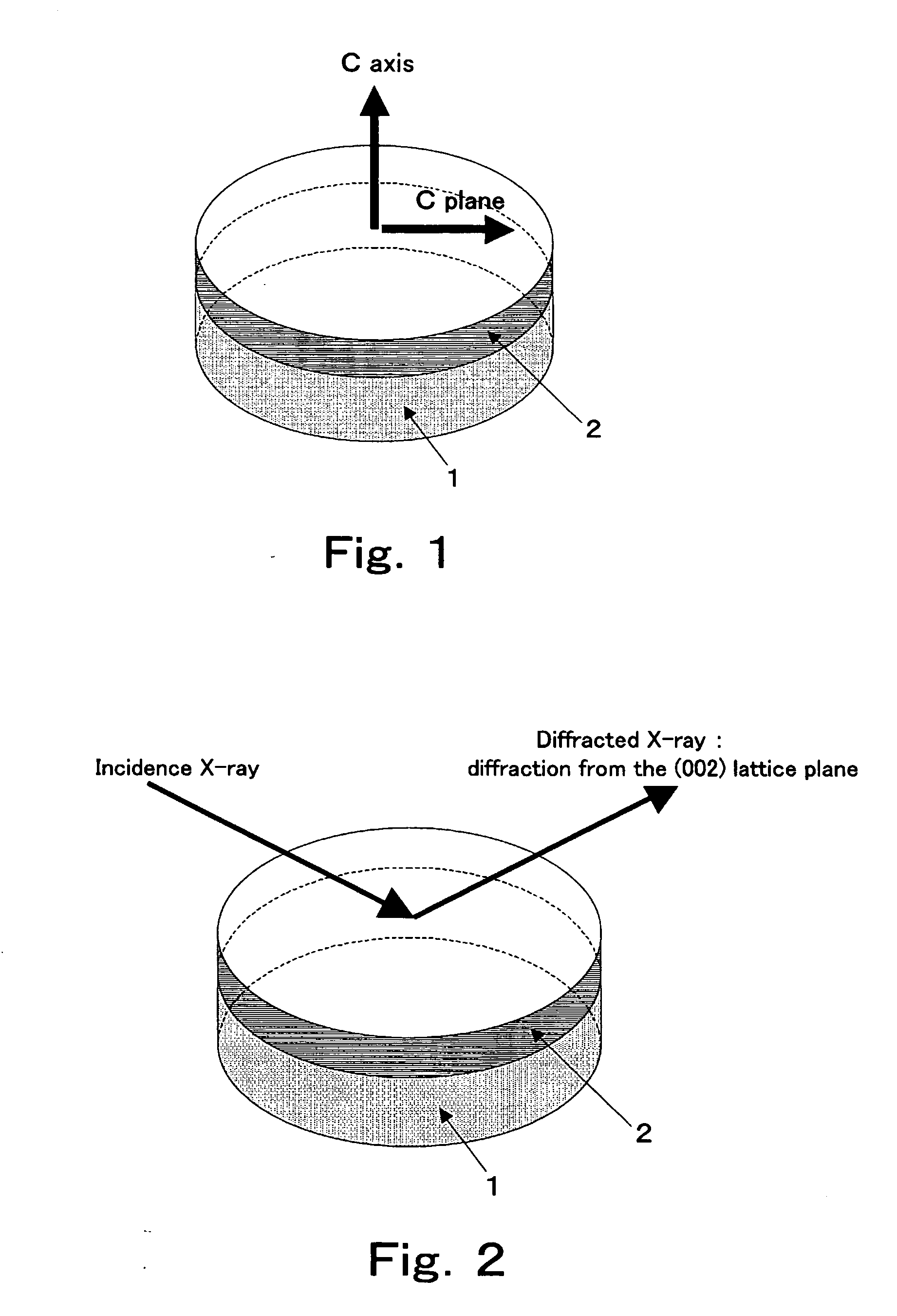
A substrate for forming a thin film composed mainly of gallium nitride, indium nitride or aluminum nitride, the substrate consisting of a sintered compact composed mainly of a ceramic material; and a thin-film substrate furnished with the thin film. The use of the sintered compact composed mainly of a ceramic material, especially translucent sintered compact, as the substrate enables formation thereon of a highly crystalline single-crystal thin film composed mainly of at least one member selected from among gallium nitride, indium nitride and aluminum nitride. Thus, there is provided a thin-film substrate furnished with a highly crystalline single-crystal thin film. Further, the use of the sintered compact composed mainly of a ceramic material enables providing of a light emitting element excelling in luminous efficiency.

Description

TECHNICAL FIELD [0001] This invention relates to a substrate for forming a thin film comprising gallium nitride, indium nitride, and aluminum nitride as a main component, a thin film substrate in which the thin film is formed, and a light-emitting device produced using the substrate. BACKGROUND ART [0002] In recent years, various light-emitting semiconductor devices, such as a light-emitting diode (LED) or a laser diode (LD), came to be used for the light source of a display, a luminaire, an optical communication, and a storage apparatus, etc. [0003] In such light-emitting semiconductor devices, a device which emits light of a green and blue color—a blue color—a purple and blue color—ultraviolet rays has been developed growing epitaxially mainly the III-V group nitride thin film comprising as a main component at least one selected from gallium nitride, indium nitride and aluminum nitride and which is constituted with at least three or more layers of the III-V group nitride single-cr...

Claims


Application Information

Patent Timeline
Patent Type & Authority Applications(United States)
IPC IPC(8): H01L33/00C04B35/453C04B35/58C04B35/581C04B35/645C30B25/18C30B29/40H01L33/32
CPCC04B35/453C04B35/58C04B35/581C04B35/645C04B2235/32C04B2235/3201C04B2235/3203C04B2235/3205C04B2235/3206C04B2235/3208C04B2235/3213C04B2235/3215C04B2235/3217C04B2235/3224C04B2235/3225C04B2235/3232C04B2235/3239C04B2235/3241C04B2235/3251C04B2235/3256C04B2235/3258C04B2235/3262C04B2235/3272C04B2235/3279C04B2235/3284C04B2235/3286C04B2235/3418C04B2235/3826C04B2235/3839C04B2235/3852C04B2235/3865C04B2235/3869C04B2235/3873C04B2235/40C04B2235/401C04B2235/402C04B2235/404C04B2235/405C04B2235/407C04B2235/408C04B2235/422C04B2235/428C04B2235/80C04B2235/96C04B2235/9607C04B2235/963C04B2235/9653C30B25/18C30B29/403C30B29/406H01L23/15
Inventor MIYAHARA, KENICHIRO
Owner MIYAHARA KENICHIRO
Learn More