

Electron-Conjugated Organic Silane Compound, Functional Organic Thin Film And Production Method Thereof
- Summary
- Abstract
- Description
- Claims
- Application Information
AI Technical Summary
Benefits of technology
Problems solved by technology
Method used
Image

Examples
experimental example 1
Preparative Example 1
Preparation of a Terphenyl Derivative Represented by General Formula (3) (A: n-octyl Group, B: Oxygen Atom, Y3: Carbon Atom, R: Hydrogen Atom, n1: 3, X1, X2, and X3: Ethoxy Group) (Hereinafter, Referred to as Terphenyl Derivative 1A (see Synthetic Route 1))
[0159] Commercially available terphenyl was used as the starting material and processed according to the synthetic route 1.
[0160] Terphenyl (cas No. 92-94-4; manufactured by Tokyo Chemical Industry Co. Ltd.) was dissolved in a solution of n-chlorosuccinimide, chloroform, and acetic acid, allowing chlorination of its terminal hydrogen. The solution in flask was stirred under a nitrogen environment, to give 4-chloroterphenyl. The 4-chloroterphenyl was dissolved in solution of sodium carbonate and sodium hydroxide in tetrahydrofuran (THF), and mixed with an excess amount of purified water. The solution was kept at 100° C. for hydroxylation of the chlorinated terminal. 4-Hydroxylterphenyl was added to and allow...
example 1
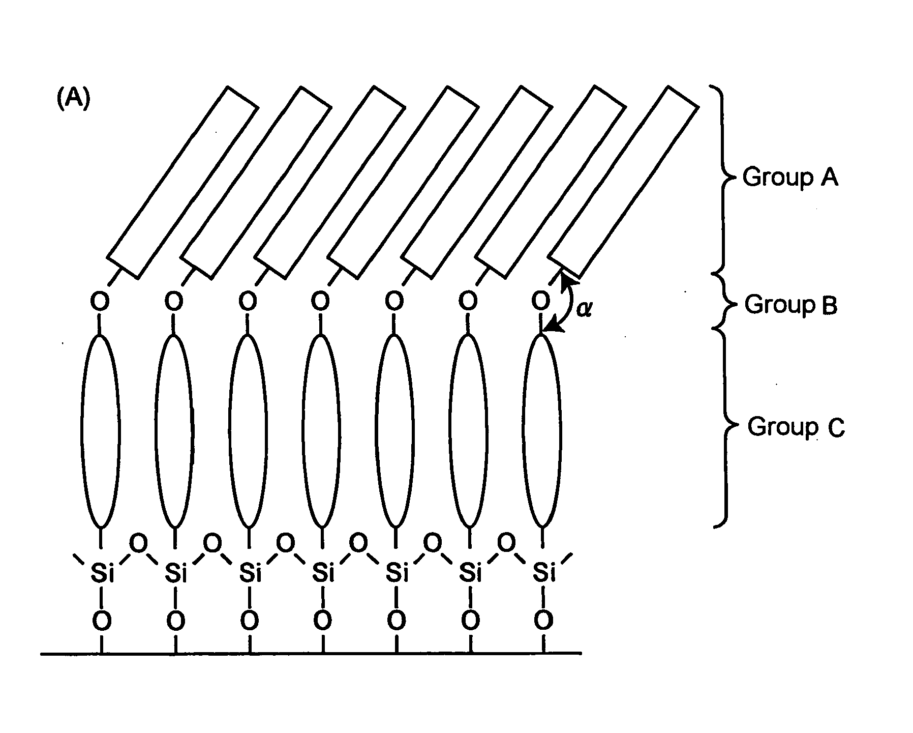
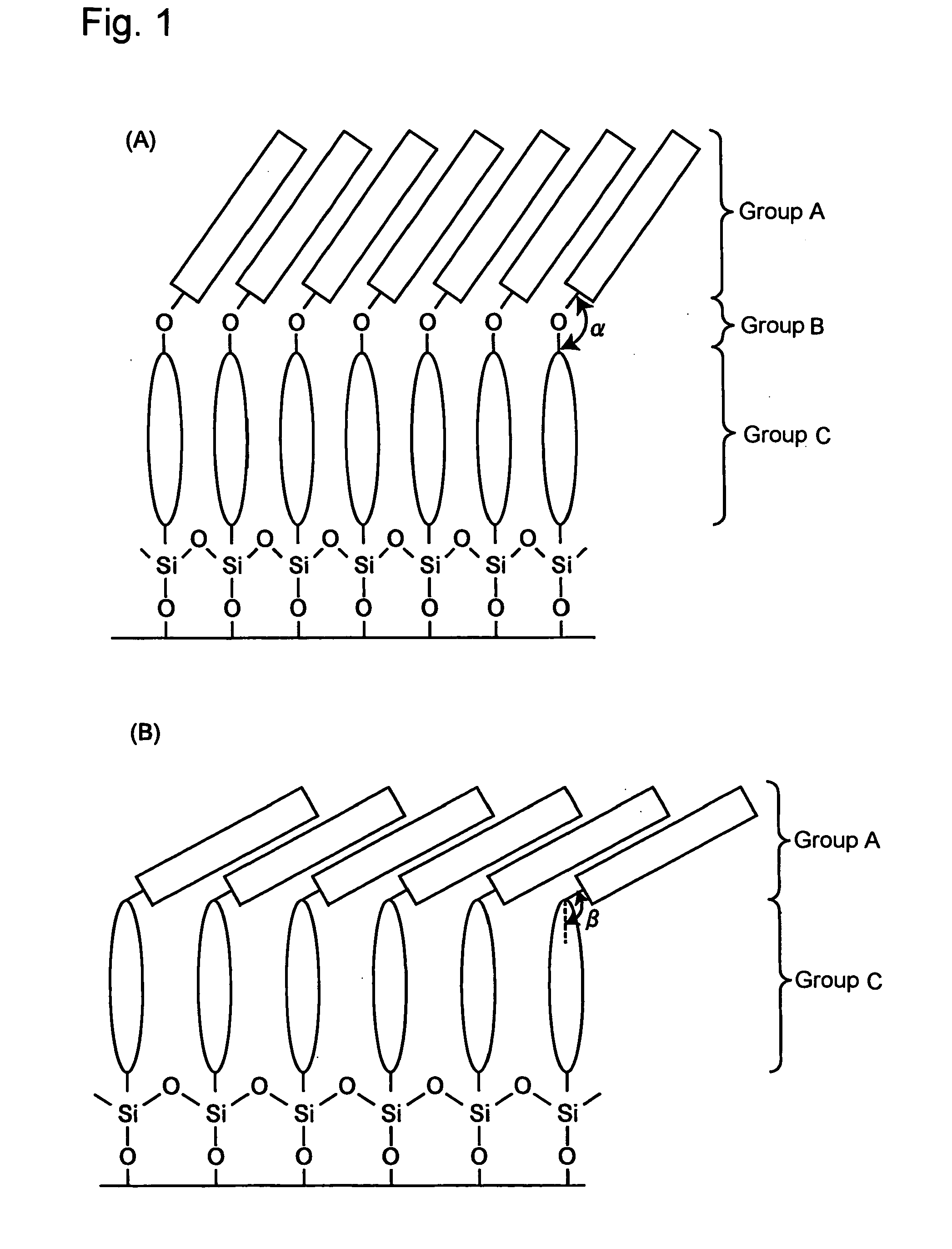
[0169] Unimolecular simulation of the terphenyl derivatives 1A and 1B by a molecular orbital method revealed that the orientation angles thereof between the terphenyl skeleton and the octyl-group bond were respectively, 161 and 140 degrees. It was possible to expand the bond orientation angle by introduction of an ether bond, indicating that it was possible to expand the orientation direction of the octyl group in the film state.
Example 2
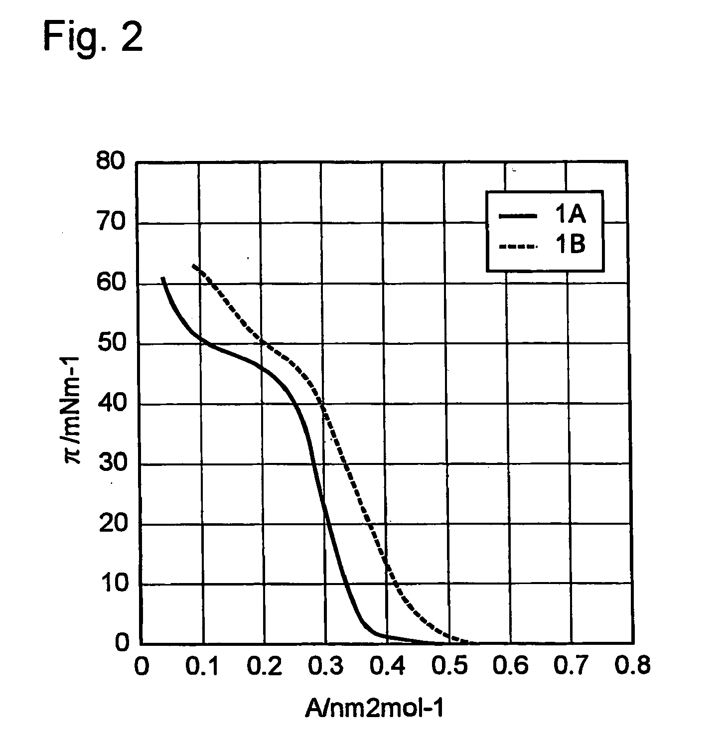
[0170] A unimolecular film of each of the terphenyl derivatives 1A and 1B was prepared by Langmuir-Blodgett (LB) method. The substrate used was a hydrophilized Si wafer. FIG. 2 shows the relationship between the surface pressure and molecular area of the film obtained by using water at pH 2 as a underlayer. The molecular area of the terphenyl derivative 1A estimated from the slope was 0.34 nm2·mol−1, while that of the terphenyl derivative 1B was 0.47 nm2·mol−1, greater than that of the terphenyl derivative 1A by approximately 0.13 nm2·mol−1. Intro...
example 2
Comparative Preparative Example 2
Preparation of a Terphenyl Derivative Represented by General Formula (1C) (Hereinafter, Referred to as Terphenyl Derivative 1C)
[0173]
[0174] A terphenyl derivative 1C having none of the octyl and ether groups was prepared for comparison.
[0175] The synthetic method used was the Grignard reaction in Preparative Example 1.
Example 4
[0176] The structural stability of the unimolecular films of terphenyl derivatives 1A and 1C was evaluated by electrical measurement. The film of terphenyl derivative 1C was prepared in a similar manner to the film in Example 2. The photoconductivity of the film was analyzed. In a similar manner to Example 2, a unimolecular film was formed on comb-tooth-shaped electrodes having a width of 200 μm respectively formed with gold and chromium in thicknesses of 30 and 20 nm by sputtering. The voltage-electric current characteristics when a 500-W Xe lamp was irradiated (bright) and not irradiated (dark) were evaluated, and the ele...
PUM
 Abstract
Description
Claims
Application Information