Eureka AIR delivers breakthrough ideas for toughest innovation challenges, trusted by R&D personnel around the world.

Topography reduction and control by selective accelerator removal

Active Publication Date: 2009-11-12
NOVELLUS SYSTEMS
View PDF101 Cites 101 Cited by
  • Summary
  • Abstract
  • Description
  • Claims
  • Application Information

AI Technical Summary

Benefits of technology

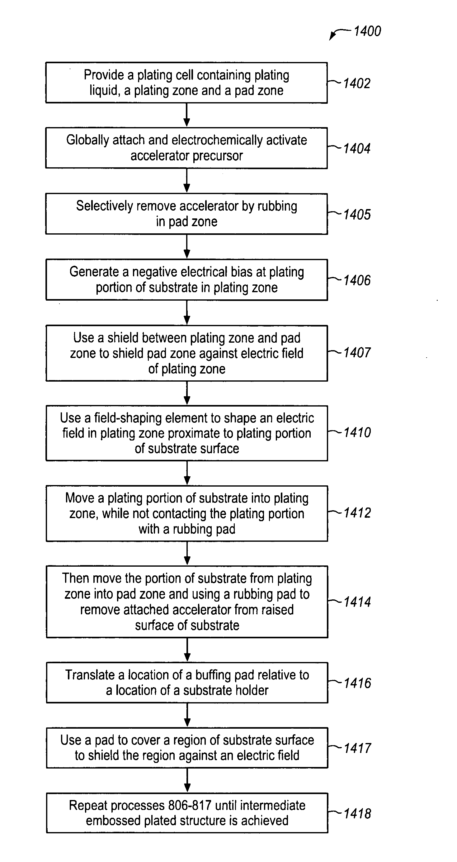
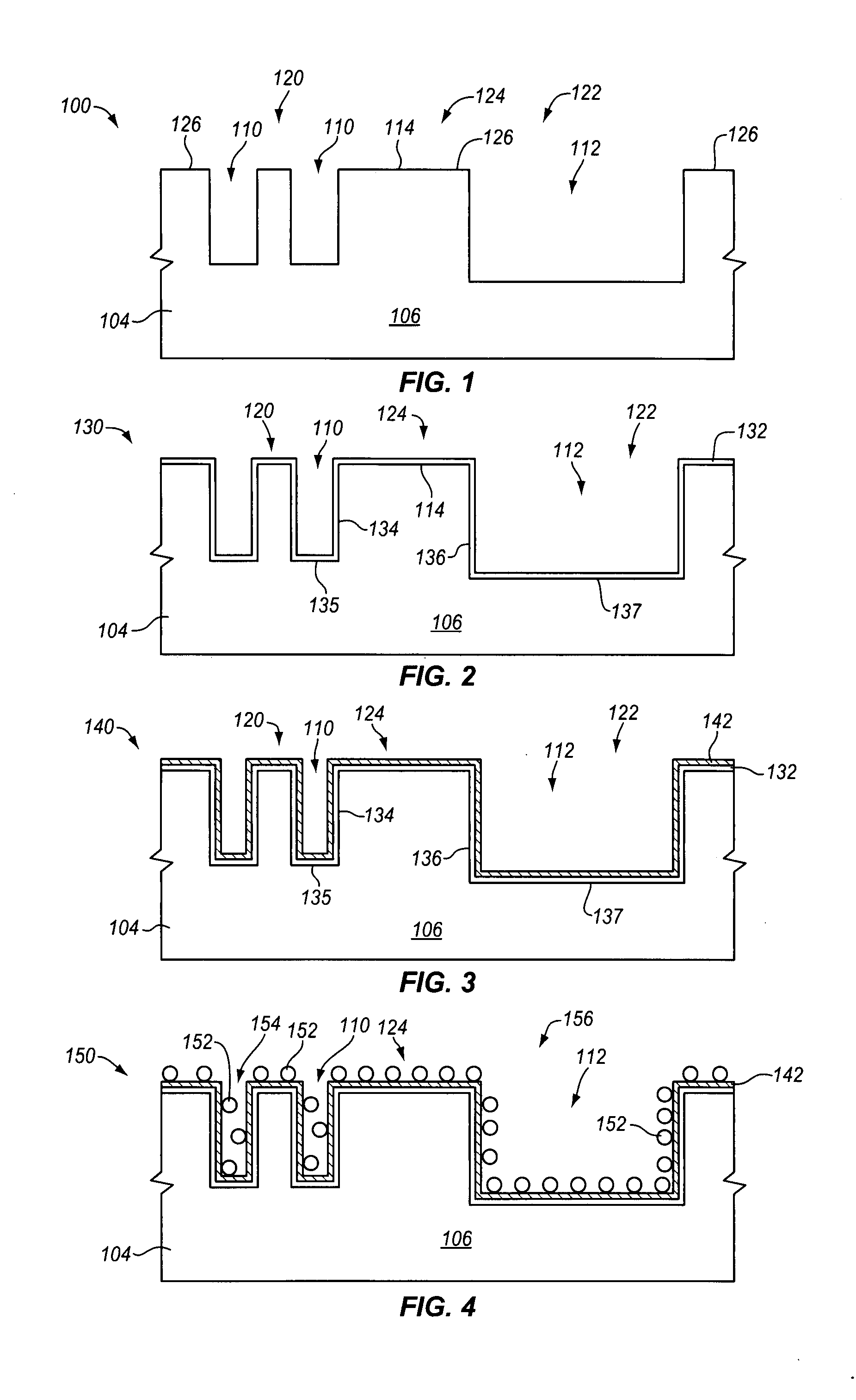
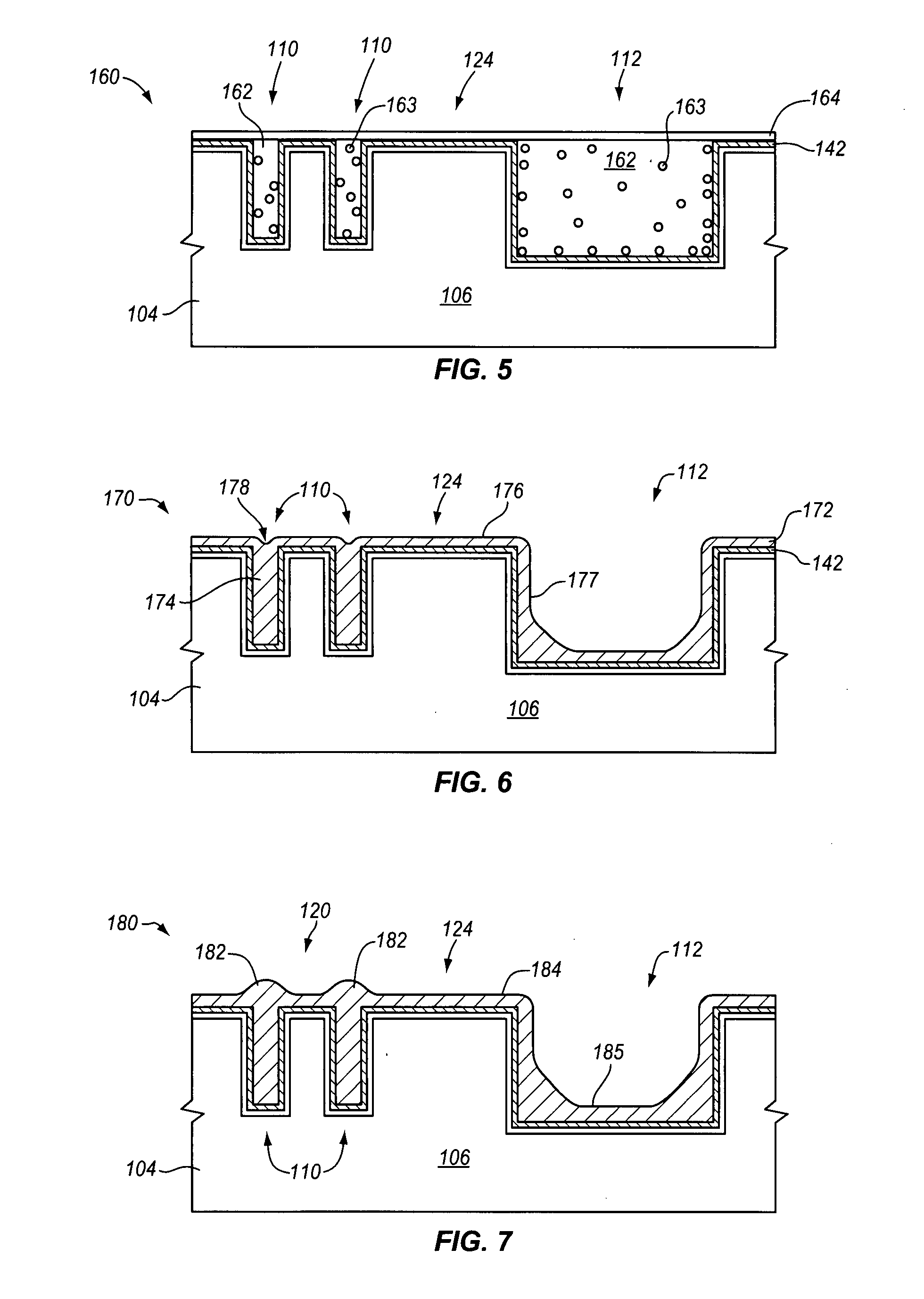
[0033]The invention helps to solve some of the problems mentioned above by providing systems, apparatuses and methods for plating and planarization of integrated circuit substrates. Some embodiments in accordance with the invention utilize selective accelerator removal (SAR) and selectively accelerated plating (SAP) of a substrate surface to produce an intermediate structure characterized by metal overburden having an “embossed” structure, on which metal protrusions above metal-filled features are higher than metal covering field regions. The metal protrusions preferably have substantially the same height. Then, the metal overburden is removed first from the field areas of the substrate and then from above the features until metal in the metal-filled features is substantially planar with a dielectric base layer. Plating and planarization in accordance with the invention avoids dishing, erosion, and scratching or other damage to metal and dielectric surfaces, while maintaining good throughput rates and minimizing costs.
[0034]Embodiments in accordance with the invention help to solve the problem of highly variable and difficult-to-control topography that commonly results from damascene copper electroplating processes. Embodiments in accordance with the invention provide “bottom-up” filling of feature cavities of all aspect ratios with minimal overburden. They enable tailoring of topography and reduction of topographic feature sizes. Some embodiments enable control of topography with little or no physical contact of hardware to a substrate surface; for example, without use of a pad or similar type of rubbing element. Methods in accordance with the invention are particularly useful in combination with various non-contacting metal removal techniques, such as isotropic wet etch, electropolishing and membrane-mediated electropolishing (MMEP). Some embodiments of methods in accordance with the invention are also useful for reducing or eliminating dishing and erosion associated with chemical mechanical polishing (CMP) operations.
[0035]Some embodiments in accordance with the invention relate to improved methods of preferentially filling features that are recessed from the general plane of the workpiece. In one aspect, some embodiments in accordance with the invention relate to a new process for improving the preferential metal-filling of high-aspect-ratio recesses (or feature cavities) (i.e., features deeper than wide). In another aspect, some embodiments relate to the reduction of excess thickness commonly observed during copper electrodeposition over a high-aspect-ratio feature (a “mound” or “bump” or excessive metal, often resulting from filling high-aspect-ratio features, sometimes called “momentum” or “overplating”). In another aspect, some embodiments in accordance with the invention relate to preferential metal-filling a recessed area (cavity) of a surface with damascene features having a low aspect ratio (i.e., features wider than deep). In another aspect, some embodiments in accordance with the invention reduce the overall amount of excess plating (overburden) on a substrate surface that typically accompanies the filling of low-aspect-ratio features.
[0036]In another aspect, embodiments in accordance with the invention relate to removal of metal from a substrate surface. In some embodiments, metal deposition and removal steps occur primarily though electrochemical or chemical action (rather than, for example, physical abrasion or sputtering), and in some embodiments, without physical contact of hardware with the surface of the substrate on which material is being deposited or from which material is being removed. The reduction and control of topography during the electroplating of copper damascene integrated circuits using the novel methods and apparatuses disclosed herein improve the filling and the control of filling of damascene features, and reduce the amount of excess metal necessary to fill recessed features. In some embodiments, it useful to continue the feature-filling processes beyond the simple filling stage (filling the recesses) to create raised or “embossed” regions over underlying features, thereby facilitating the use of preferred removal process sequences, such as a non-contacting wet etch (preferably a surface-reaction-controlled feature-size-independent isotropic wet etch) or membrane-mediated electropolishing (MMEP). Intermediate structures having excess metal above metal-filled features are referred to as being “proud”, “embossed” or with protrusions. The protection of underlying metal-filled features with excess metal above the features helps reduce undercutting, dishing, and erosion, helps enhance substrate planarization steps (e.g., barrier / dielectric CMP) after plating, and helps reduce the impacts of underlying topography in subsequent device level manufacture.
[0037]Some embodiments in accordance with the invention utilize membrane-mediated elements to achieve electrochemical oxidization and planarization without having to make physical ohmic contacts to the substrate surface. Membrane-mediated elements also help to avoid well-known terminal effect phenomena (ohmic-resistance current distribution problems in thin metal layers).
[0038]Methods in accordance with the invention allow use of a simple, low-cost isotropic wet-etching technique after metal plating that selectively removes remains of copper and typically is stopped at a barrier / etch-stop layer. A feature of some embodiments of methods in accordance with the invention is the capability of planarizing the entire surface of the substrate face, including extreme peripheral portions of the substrate face contiguous to the side edges of the substrate.

Problems solved by technology

As the number of levels in an interconnect technology is increased, the stacking of additional layers produces more rugged and complex topography.
Baths with good “bottom-up” filling characteristics fill high aspect ratio features more rapidly and without creating void or seam when compared to baths with less effective combinations of such additives.
The use of advanced “bottom-up” electrofilling techniques with wafers having low and high aspect-ratio features has created a problem of deposited metal surfaces with a wide range of topography, that is, topography containing a large range of height and width variations in both recessed and raised areas.
Therefore, while electroplating is the preferred method of metallization, various aspects of improved plating regimens create challenging topography for subsequent planarization
These approaches and techniques generally require overburden.
Overburden is undesirable for a number of reasons.
It requires deposition of considerable amounts of excess copper that is essentially wasted.
Thus, overburden represents additional materials costs (excess copper deposited and removed), as well as decreased throughput and productivity.
CMP and eCMP are particularly expensive processes that generally use corrosive chemical and slurry formulations on large (wafer scale or larger) pads to polish the surface of the integrated circuit substrate.
Such pad-rubbing processes are often difficult to control and the polishing end-point can be difficult to detect.
The high equipment cost, waste handling cost, and low throughput contribute to the overall expense of CMP and eCMP.
Also, with the introduction of porous low-k dielectrics in semiconductor devices, modification of traditional CMP and even eCMP processes is required, as current methods can crack and / or delaminate low-k materials, which typically have a very low compression strength and extreme fragility.
Furthermore, none of these techniques achieve perfect planarization.
The large downward pressure exerted onto a wafer during typical CMP polishing may damage fragile low-k dielectrics.
While multilayer laminated pads containing materials of variable compliance (stiffer layer near the interface, more compliant layers further away from the interface) help address some mechanical tolerance requirements, it is well know that CMP and eCMP techniques suffer from substantially non-ideal planarization performance and global non-uniformities.
As a result of CMP technology's inability to achieve perfect die-level planarization, and because of global wafer-scale height variations, excess processing (beyond the point where metal over the field around the feature has been completely removed) occurs on certain areas than would otherwise be desirable.
Hence, substantial overpolishing over some feature types (typically larger features) and parts of the wafer occurs.
A difficult problem of CMP includes defect generation and scratching of fine-lined metal in dielectric features by foreign particles as well as the agglomerations of abrasive particles.
Scratching results in damage to interconnects and reduces device manufacturing yield.
A conglomerate of particles and gels can be removed from the slurries using point-of-use filtration prior to substrate polishing; however, plugging of the filters requires interruption of the process for filtrate removal, which is expensive and results in lower production.
Because neither the metal deposition (e.g., electroplating) nor metal removal (e.g., CMP) processes are perfectly uniform across the wafer surface, global non-uniformities also exist.
The problem then arises that the interconnect metal (e.g., copper) in the feature is slowly removed, preferentially in the feature, hence “dished”.
During the subsequent CMP of barrier / dielectric material, the risk of erosion arises.
The overall deviations from planarity caused by dishing, erosion, and underlying topography can also lead to difficulties in obtaining good focus across the die during subsequent lithographic steps.
These areas are particularly troublesome for CMP technology because of the competing requirements of having planarization and compliance.
Often CMP has difficulty clearing metal from recessed areas of underlying topography, leaving “puddles” of metal.
To remove these puddles, the CMP process is generally continued for a longer period of time than otherwise desirable (because this can create excessive dishing).
While etching (electroless etching), electropolishing, electrochemical etching, and membrane mediated electropolishing processes are simpler, less costly operations than CMP (and eCMP), they generally have a more limited ability to planarize a “contoured” surface over longer planarization lengths (either wider features or over longer distances).
Nevertheless, a problem arises during the electropolishing of surfaces in which a large number of low aspect-ratio (larger width than depth) features exist.
Depositing a thick metal layer would be uneconomical due to necessary removal of the large excess of metal at a later stage.
This is an unacceptable result.
Similar problems may arise from chemical (nonelectrolytic) wet etching of metal from a substrate surface.
Furthermore, if chemical wet etching were conducted long enough to remove substantially the metal over the field areas and above “overplated” high-aspect-ratio features of a nonplanar substrate, then excessive over-etching of metal and generation of recesses in low-aspect-ratio features would result.
However, due to their physical and geometrical limitations, these processes are not capable of filling low-aspect-ratio features (e.g., contact pads).
It is known that the use of a rubbing element, such as a pad, in continuous moving contact with a surface such as a wafer creates problems (e.g., defects, feature damage, plating protrusions, metal particle deposition on the pad, and contamination of deposited metal by pad material), and the influence of adsorption dynamics (diffusion, surface reaction rates, local consumption rates, etc.) can make process control difficult.
Furthermore, plating selectivity between recessed and exposed regions is generally less than optimal because a finite rate of additive re-adsorption tends to reduce the plating selectivity.
The mechanism of masked plating, and specifically the role of a mask-plating pad in creating differential plating activity, remains unclear and leads to doubt regarding optimization, a method's robustness, and its overall utility.
In addition, while the desired properties of pads have not been specified clearly, the effects of continual contact of a pad with the substrate surface and of the associated continual wear require significant pad conditioning to maintain performance and selectivity.
This substantially limits the overall pad life and process flexibility.
Replacement of the mask plating pad is not only potentially costly from a material standpoint, but also from a tool utilization and uptime standpoint.

Method used


Image

  • Topography reduction and control by selective accelerator removal
  • Topography reduction and control by selective accelerator removal
  • Topography reduction and control by selective accelerator removal

Examples


example 1

[0242]Accelerator removal tests were performed on a central section of a number of 300 mm thermal-oxide coated silicon wafers using an apparatus 800 as depicted in FIG. 39. Each silicon wafer had a 150 Å tantalum barrier / adhesion layer and a 1000 Å copper PVD seed. Each wafer was “pre-electroplated” in a SABRE® plating tool available from Novellus Systems, Inc. The pre-electroplating was performed at a charge density of 0.32 C / cm2 (at approximately 1200 Å) in a copper plating bath containing additives and electrolytes for filling 35 nm narrow-cavity features having an aspect ratio exceeding 4:1. The pre-plating step is useful for simulating and elucidating the abrasion interactions between a pad and the metal micro-topography and roughness that generally are present on a surface after a narrow-feature (HAR) metal deposition / filling operation. Prior to global accelerator application, the wafer was etched (etch rate about 1000 Å / min) to remove residual plating bath adsorbates / levelers...

example 2

[0268]Localized metal etching in accordance with the invention was performed to remove copper from a series of 200 mm semiconductor wafers using an etching solution in accordance with the invention together with a diluent (deionized water) or one of various quenching solutions. Liquid etchant was dispensed onto a wafer that was rotating at 500 rpm at a location about 50 mm from the wafer center. The liquid etchant was dispensed for 30 seconds at a flow rate of 40 milliliters per minute (ml / min) through an applicator nozzle having a diameter of 0.02 inches (0.51 mm). The etchant liquid comprised an etching solution containing 5 g / L of 30 weight percent (wt %) H2O2 and 4 g / L glycine. Concurrently, diluent or quenching liquid was dispensed for 30 seconds at a flow rate of 150 ml / min through a quench nozzle having a diameter of 0.03 inches (0.76 mm). The quench nozzle was located next to the etchant applicator nozzle, 0.43 inches (about 11 mm) radially outwards from the applicator nozzl...

example 3

[0270]A localized etching procedure in accordance with the invention was conducted to remove copper from 200 mm semiconductor wafers under conditions similar to those described above in Example 2 to demonstrate the effect of diluent flowrate on localized copper removal.

[0271]As in Example 2, liquid etchant was dispensed onto a wafer that was rotating at 500 rpm at a location about 50 mm from the wafer center. The liquid etchant was dispensed for 30 seconds at a flow rate of 40 ml / min through an applicator nozzle having a diameter of 0.02 inches (0.51 mm). The etchant liquid comprised an etching solution containing 5 g / L of 30 weight percent (% wt.) H2O2 and 4 g / L glycine. Concurrently, deionized water was dispensed for 30 seconds at a flow rate of 2700 ml / min through a quench nozzle having a diameter of 0.156 inches (4.0 mm). The quench nozzle was located next to the etchant applicator nozzle, 0.43 inches (about 11 mm) radially outwards from the applicator nozzle.

[0272]After applica...


PUM

PropertyMeasurementUnit
Areaaaaaaaaaaa

Abstract

Plating accelerator is applied selectively to a substantially-unfilled wide (e.g., low-aspect-ratio feature cavity. Then, plating of metal is conducted to fill the wide feature cavity and to form an embossed structure in which the height of a wide-feature metal protrusion over the metal-filled wide-feature cavity is higher than the height of metal over field regions. Most of the overburden metal is removed using non-contact techniques, such as chemical wet etching. Metal above the wide feature cavity protects the metal-filled wide-feature interconnect against dishing, and improved planarization techniques avoid erosion of the metal interconnect and dielectric insulating layer. In some embodiments, plating of metal onto a substrate is conducted to fill narrow (e.g., high-aspect-ratio feature cavities) in the dielectric layer before selective application of plating accelerator and filling of the wide feature cavity.

Description

RELATED APPLICATIONS[0001]This application is a divisional application, claiming priority under 35 USC § 120 and 37 CFR 1.53(b) of co-owned and co-pending U.S. patent application Ser. No. 11 / 602,128, filed Nov. 20, 2006, by Mayer et al., which claims the benefit under 35 USC 119(e) of U.S. Provisional Application Ser. No. 60 / 737,978, filed Nov. 19, 2005, by Mayer et al. This application is also a continuation-in-part application, claiming priority under 35 USC 120, of co-owned and co-pending U.S. patent application Ser. No. 11 / 544,957, filed Oct. 5, 2006, by Mayer et al., which claimed the benefit of U.S. Provisional Application Ser. No. 60 / 724,209, filed Oct. 5, 2005, titled “Selective Electrochemical Accelerator Removal”. This application is a continuation-in-part application, claiming priority under 35 USC 120, of co-owned and co-pending U.S. patent application Ser. No. 10 / 824,069, filed Apr. 13, 2004, by Drewery et al., having the title “Selectively Accelerated Plating of Metal ...

Claims


Application Information

Patent Timeline
IPC IPC(8): H01L21/44C25D17/00H01L21/306
CPCB23H5/08C25D17/14C25D17/06C25F3/16C25F3/30H01L21/02068H01L21/2885H01L21/32115H01L21/3212H01L21/32134H01L21/7684H01L21/76849H01L21/76877C25D7/123C25D5/06C25D17/001C25D5/08C25D5/02C25D5/34
Inventor MAYER, STEVEN T.REA, MARK L.HILL, RICHARD S.KEPTEN, AVISHAISTOWELL, R. MARSHALLWEBB, ERIC G.
Owner NOVELLUS SYSTEMS
Why Eureka
Eureka Blog
Learn More