Visible-to-Longwave Infrared Single Photon Avalanche Photodetector on Silicon

a single-photon avalanche and photodetector technology, applied in the direction of diodes, semiconductor devices, radio-controlled devices, etc., can solve the problems of bump bonding requirement, high reliability, and inability to focus, so as to reduce timing jitter, reduce reverse leakage current, and high fill factor

Pending Publication Date: 2021-11-04
SEMIKING LLC
View PDF1 Cites 0 Cited by
  • Summary
  • Abstract
  • Description
  • Claims
  • Application Information

AI Technical Summary

Benefits of technology

[0018]A second SPAD device structure embodiment is disclosed where the p-n junction intersects with the dielectric on the top surface. The top Ge / oxide interface is more easily treated to minimize traps and demonstrates an overall lower dark current at the cost of a reduction in fill factor. In addition, due to placement of the p-n junction, both lateral and vertical electric fields act to divert dark generated carriers from entering the multiplication zone and thus lower the DCR. Unlike the embodiment already discussed, the first p-type implant in this structure acts as a conventional guard ring and is lithographically patterned with its edge displaced from the single crystal growth / oxide boundary by an amount depending on the doping levels and Ge region thickness. The second p-type implant is performed with a circularly patterned mask placed within the area of the first implant to define the avalanche multiplication region as in the first embodiment. N-type implants along the length of the single crystal grown perimeter region prevent depletion from negative charge that may be present at the Ge / oxide interface. Finally, to obtain an additional lever to control the semiconductor surface potential, a gate is placed above the guard ring to help minimize dark current generation and prevent premature breakdown along the device perimeter.
[0020]A third embodiment of our invention is an avalanche photodiode structure that uses the dislocation free semiconducting region to form a multiplication zone and an epitaxial layer of a smaller bandgap material subsequently grown on top to serve as an absorptive layer. The resulting separate absorption and multiplication (SAM) structure permits the depletion region to exist primarily within the larger bandgap material thus reducing the reverse leakage current. The separate absorption layer decreases timing jitter since electron-hole pairs are created almost exclusively within that layer. This structure will also serve as a detecting element even if it is not biased into breakdown for certain epitaxial layer compositions as may be useful for MWIR and LWIR imaging.
[0021]Our SPAD design allows a high fill factor providing for a high PDE in the device. The SPAD designs according to our invention keep DCR low by making sure many surface generated dark carriers are collected in areas of the device with intentionally low impact ionization probabilities. At the same time, very thick depletion regions are possible in the design which will favor impact ionization over band-to-band tunneling. Thus, DCR mechanisms that are known to dominate many small area, low band gap SPADs are managed advantageously in our design.

Problems solved by technology

This ability to focus poses an inherent danger to human sight if the laser illumination levels used in the LiDAR system exceed the maximum permissible exposure (MPE).
For most infrared imagers, this bump bonding requirement comes about because today's photodetectors use compound semiconductor materials such as InGaAs, InSb, and HgCdTe that are largely incompatible with silicon processing.
The resultant hybrid image sensor formed by this bonding process exhibits problems with reliability, semiconductor manufacturing yield, chip size, and most importantly high cost.
The size of the indium bump itself limits pixel dimensions thus electronic innovations accomplished in related fields such as CMOS scaling cannot be used to their fullest extent.
Germanium has a 4 percent lattice mismatch to silicon rendering a highly defective layer when epitaxially grown directly on silicon.
Minority carrier p-n junction devices fabricated in this Ge material possesses very high dark current and thus high noise.
The high noise of these devices makes them useless for photon starved applications like low light imaging and high performance LiDAR.
To date these materials use a heavily defective Ge buffer layer on Si, the resulting quality of the subsequently grown SiGeSn and GeSn layers are also heavily defective and not useful for device applications where low reverse (dark) current is essential.
While a simple photodetector using these nearly defect free semiconductor regions yields low dark current, it does not have enough sensitivity for long range LiDAR applications.
A disadvantage of many guard ring designs is that the area requirement of the device is significantly larger than the central heavily doped p-type region area.
This disadvantage may be particularly pronounced for higher voltage designs with overall lower doping levels.
In addition, metallization is needed to connect to the well, causing optical shadowing effects for front-side illuminated devices employing common guard ring designs.
For small pixel pitch devices, the disadvantages of a guard ring design becomes more severe, which has prompted work on vertical Si SPAD designs and Si SPAD designs with guard ring areas overlapping with dielectric isolation structures.

Method used


Image

  • Visible-to-Longwave Infrared Single Photon Avalanche Photodetector on Silicon
  • Visible-to-Longwave Infrared Single Photon Avalanche Photodetector on Silicon
  • Visible-to-Longwave Infrared Single Photon Avalanche Photodetector on Silicon

Examples


fourth embodiment

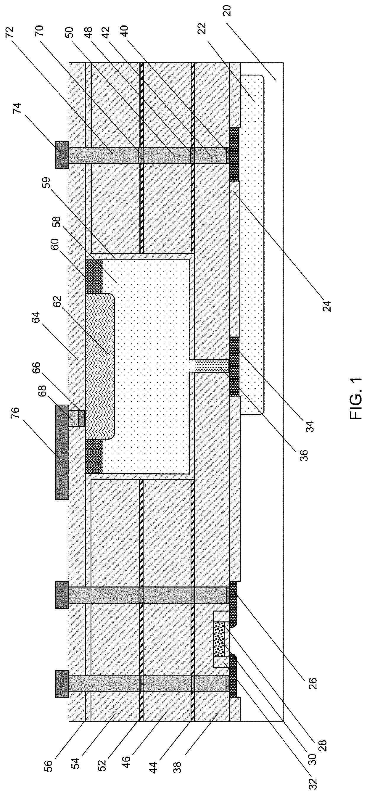
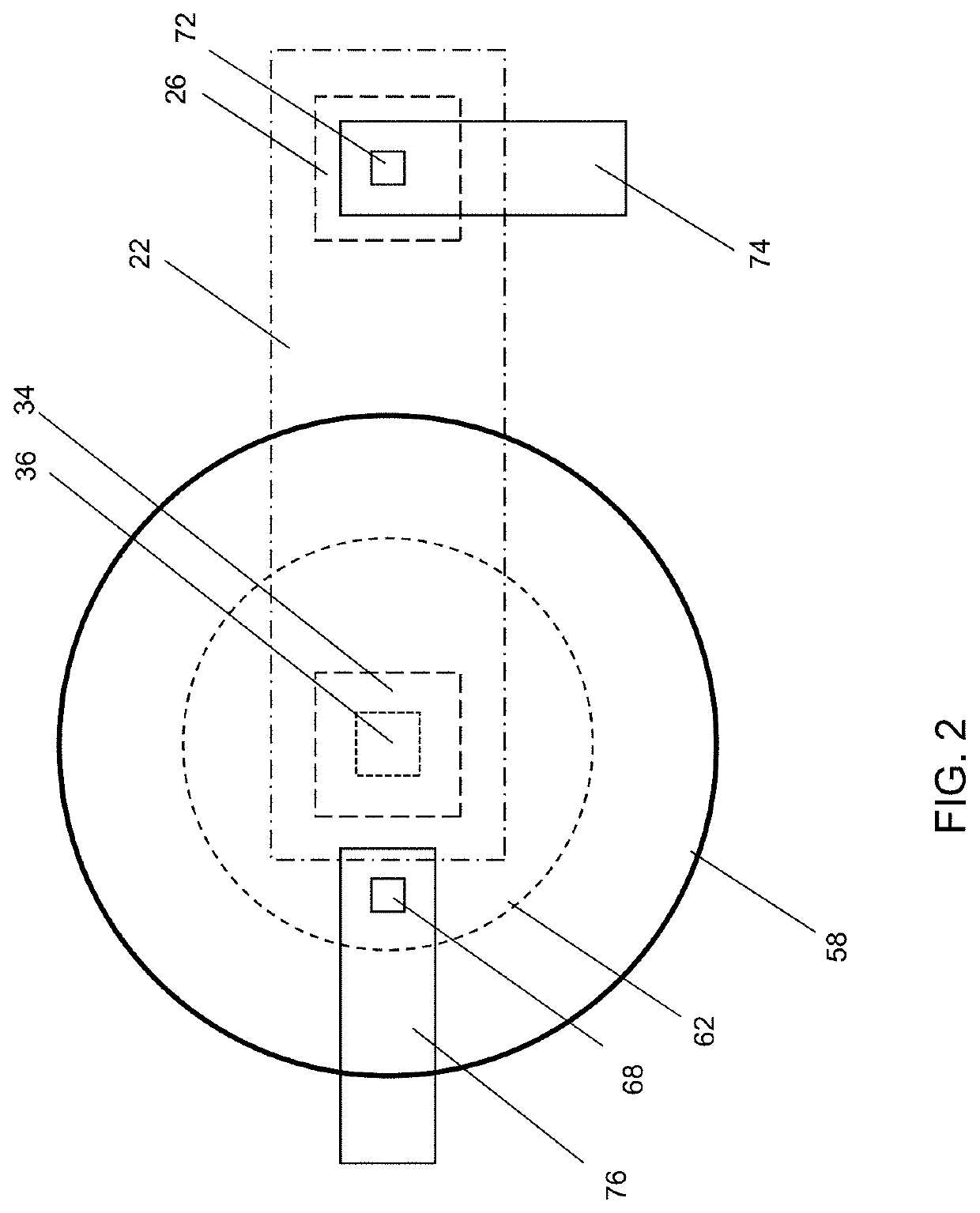
[0016]Three device structures are disclosed to produce a high performance SPAD in embodiments of the present invention. A fourth embodiment describes opaque elements added around the periphery of the device to prevent cross-talk between pixels. Two of the device structures differ in their placement of the heavily doped p-type region relative to the dielectric isolation. The third device employs a separate absorption and multiplication (SAM) structure using different materials for each region. To form the important doped regions of the Ge SPAD device, ion implantation and subsequent annealing of the resulting damage may be used as well known to those skilled in the art. To protect the sensitive semiconductor surface from contamination during photolithography and ion implantation steps, a thin screen oxide may be deposited on the single crystal Ge surface. Blanket phosphorous implants without any photolithographic patterning ensure the entire Ge region above the seed trench region is ...

first embodiment

[0017]The first embodiment employs four p-type implants to form the SPAD anode to create a high fill factor device. To make this SPAD, two p-type blanket implants are performed without photolithographic patterning to span a region at the top of the device to all the dielectrically isolated edges. Next, two more p-type implants are performed with a circular or near-circular lithographically formed pattern centered within the single crystal grown region. These implants have a higher dose and extend deeper into the device than the previous implants and define a perimeter of the multiplication region of the device. The multiplication region of the device extends below the p-type implants into the semiconductor region. The p-n junction of this embodiment intersects with the oxide isolation sidewall defining the nearly defect free grown region. The electric field at the breakdown voltage is high in the central region and is immediately reduced at the edge of the p-type doped region define...

third embodiment

[0020]our invention is an avalanche photodiode structure that uses the dislocation free semiconducting region to form a multiplication zone and an epitaxial layer of a smaller bandgap material subsequently grown on top to serve as an absorptive layer. The resulting separate absorption and multiplication (SAM) structure permits the depletion region to exist primarily within the larger bandgap material thus reducing the reverse leakage current. The separate absorption layer decreases timing jitter since electron-hole pairs are created almost exclusively within that layer. This structure will also serve as a detecting element even if it is not biased into breakdown for certain epitaxial layer compositions as may be useful for MWIR and LWIR imaging.

[0021]Our SPAD design allows a high fill factor providing for a high PDE in the device. The SPAD designs according to our invention keep DCR low by making sure many surface generated dark carriers are collected in areas of the device with int...


PUM


Abstract

A single photon avalanche (SPAD) device configured to detect visible to infrared light includes a substrate and a trench coupled to the substrate. The trench has a lattice mismatch with the substrate and has a height equal to or greater than its width. The device further includes a substantially defect-free semiconductor region that includes photosensitive material. The semiconductor region includes a well coupled to the trench and doped a first type. The well is configured to detect a photon and generate a current. The semiconductor region also includes a region formed in the well and doped a second type opposite to the first type. The well is configured to cause an avalanche multiplication of the current. The trench and the well form a first electrode and the region forms a second electrode.

Description

CROSS REFERENCE TO RELATED APPLICATIONS[0001]The present application is a continuation-in-part of U.S. patent application Ser. No. 17 / 244,135 filed Apr. 29, 2021, which claims the benefit of U.S. Provisional Patent Application No. 63 / 017,292 filed Apr. 29, 2020, U.S. Provisional Patent Application No. 63 / 033,315 filed Jun. 2, 2020, and U.S. Provisional Patent Application No. 63 / 117,631 filed Nov. 24, 2020, the disclosures of which are incorporated by reference herein in their entirety.BACKGROUND OF THE INVENTIONField of the Invention[0002]This invention relates to a single photon avalanche photodetector fabricated on a silicon wafer that is sensitive from the visible to longwave infrared spectral regions.Discussion of the Related Art[0003]Image sensors capable of creating images in the infrared spectral region are important in a wide variety of applications including fiber optic communications, light detection and ranging (LiDAR), fluorescence lifetime imaging microscopy (FLIM), sil...

Claims


Application Information

Patent Timeline
Patent Type & Authority Applications(United States)
IPC IPC(8): H01L27/146
CPCH01L27/1461H01L27/14643H01L31/0312H01L27/14623H01L27/14603H01L31/107H01L27/14612H01L27/1463H01L31/1808H01L31/02327
Inventor KING, CLIFFORD ALANABERG, ANDERS INGVAR
Owner SEMIKING LLC
Why Eureka
Try Eureka