

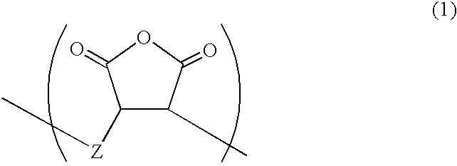
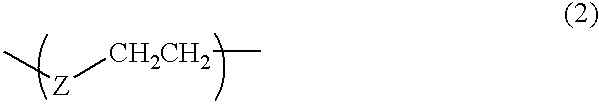
Resist resin, chemical amplification type resist, and method of forming of pattern with the same
a technology of resist and resist pattern, which is applied in the direction of photosensitive materials, instruments, photomechanical equipment, etc., can solve the problems of difficult to obtain excellent resist pattern, cost performance, and high cost of laser beam machines, and achieve excellent adhesion to substrates, excellent dry etching resistance and transparency, and high pattern resolution
- Summary
- Abstract
- Description
- Claims
- Application Information
AI Technical Summary
Benefits of technology
Problems solved by technology
Method used
Image


Examples
synthesis example 1
Norbornene derivative represented by formula (19) (Endo form)
[0076]12.8 g of sodium boron hydride was added to 100 ml of tetrahydrofuran (hereinafter abbreviated to THF). Thereto was dropwise added, with ice-cooling, a solution of 50 g of 5-norbornene-endo-2,3-dicarboxylic acid anhydride (No. 146-03435, a product of Wako Pure Chemical Industries, Ltd.) dissolved in 200 ml of THF. The resulting mixture was stirred at room temperature for 3 hours. Then, 150 ml of 6 N hydrochloric acid was added with ice-cooling, followed by stirring at room temperature for 3 hours. The resulting precipitate was removed by filtration. The filtrate was concentrated under vacuum. To the residue was added 300 ml of chloroform. Thereto was added silica gel to remove impurities by adsorption. The resulting solution was subjected to distillation under reduced pressure to remove chloroform to obtain 16.5 g (yield: 36%) of an intended product.
[0077]1H-NMR (CDCl3): δ (ppm) 1.47 (1H,dd), 1.65 (1H,d), 3.06-3.15 (...
synthesis example 2
Norbornene derivative represented by formula (19) (Exo form)
[0078]100 g of 5-norbornene-endo-2,3-dicarboxylic acid anhydride was subjected to a reaction in a nitrogen atmosphere at 190 to 195° C. for 4 hours. The reaction mixture was allowed to cool and then recrystallized with toluene 5 times to obtain 28 g (yield: 28%) of 5-norbornene-exo-2,3-dicarboxylic acid anhydride. This 5-norbornene-exo-2,3-dicarboxylic acid anhydride was reduced by the same procedure as in Synthesis Example 1, to obtain an intended product (yield: 49%).
[0079]1H-NMR (CDCl3): δ (ppm) 1.39-1.58 (2H,m), 2.47-2.71 (2H,m), 2.89 (1H,s), 3.25 (1H,s), 3.95-4.03 (1H,m), 4.42-4.53 (1H,m), 6.1-6.35 (2H,m)
synthesis example 3
Norbornene derivative represented by formula (21) (Endo form, R is methyl group)
[0080]Synthesis was conducted in the same manner as in Synthesis Example 1 except that the 5-norbornene-endo-2,3-dicarboxylic acid anhydride was replaced by methyl-5-norbornene-endo-2,3-dicarboxylic acid anhydride (No. 136-05955, a product of Wako Pure Chemical Industries, Ltd.) (yield: 33%).
PUM
| Property | Measurement | Unit |
|---|---|---|
| wavelength | aaaaa | aaaaa |
| wavelength | aaaaa | aaaaa |
| wavelength | aaaaa | aaaaa |
Abstract
Description
Claims
Application Information