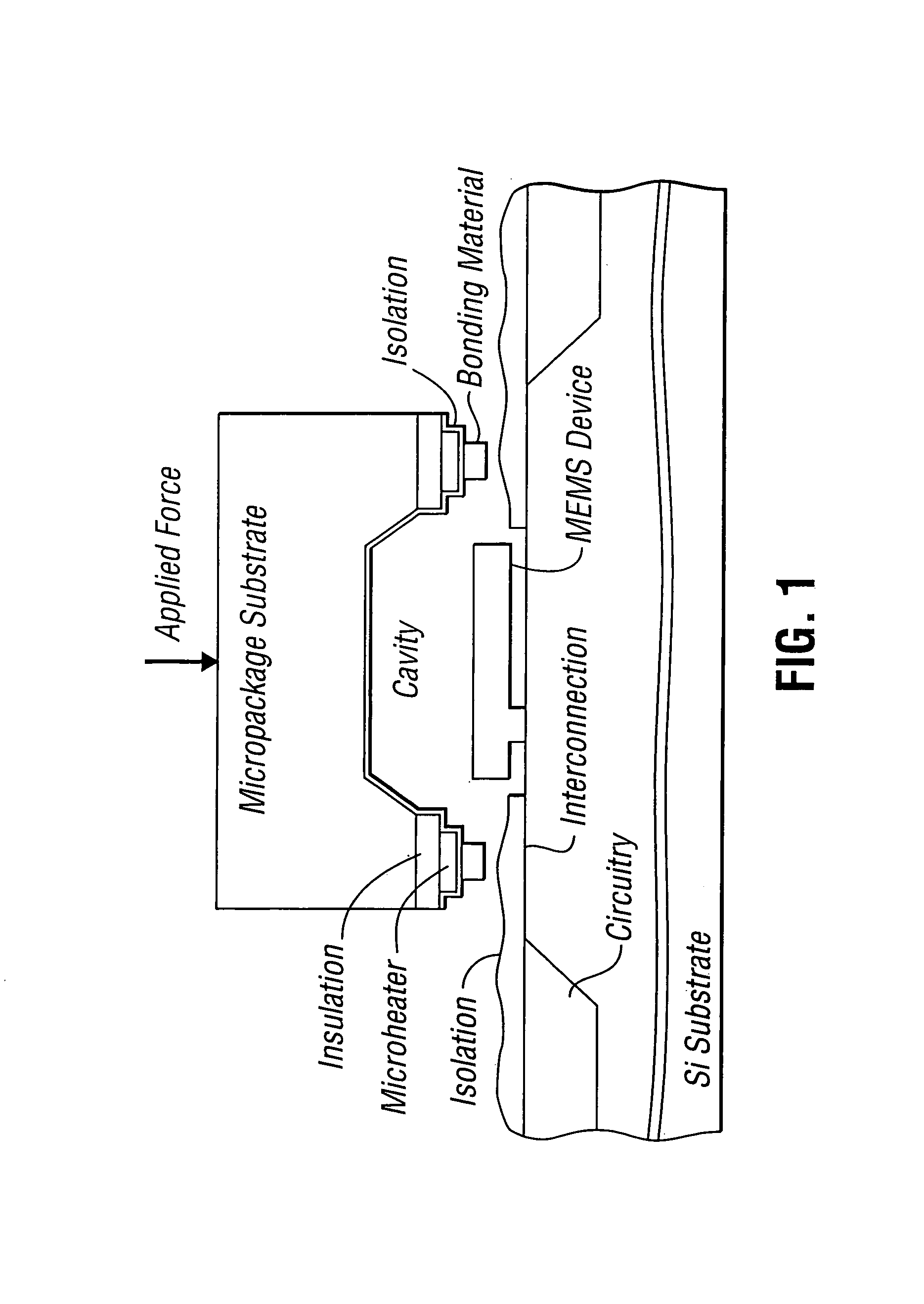
The manufacture of MEMS devices, such as micro-gyroscopes, micro-accelerometers, resonant accelerometers, micro-mirrors, micro-motors, micro-actuators and other such micro-devices integrating at least one moving part presents a very serious challenge in terms of packaging.
Since such MEMS devices are typically fabricated from the combination of various materials having different coefficients of
thermal expansion, it is important to minimize the
exposure of the MEMS devices to high temperatures since this released component may be affected by the mechanical effects resulting from these various coefficients of
thermal expansion Such effects can be observed as out-of-specification sensing or actuation, induced flexion and ultimately
stiction between the released component and its surrounding materials, induced mechanical stress or mechanical failures in the released component, and unreliable performance in the field.
Such an upper limit of 400° C. clearly limits the use of the well known direct
wafer bonding (DWB) technique, which requires a temperature of about 1000 to 1200° C. to bond two polished
silicon surfaces.
Unfortunately, none of these processes satisfy all the requirements for these special situations.
Pyrex™ 7740 glass contains a lot of
sodium in the form of Na2O and is thus absolutely incompatible with a
CMOS line of products.
This very serious limitation implies that the fabrication MEMS devices using in accordance with this reference must be limited to a dedicated tool set and cannot simply be introduced into a standard
CMOS production line.
Moreover, it also implies that this cited Pyrex-based wafer-level packaging technique will limit the development of future MEMS devices integrating optional sensing, control or communication devices and optional high-
voltage actuation drivers.
While this patent requires the use of undesirable glasses, the process described is carried out at an excessive local temperature
ranging between 820° C. and 1300° C., which may cause undesirable mechanical
stress gradient in the surrounding structures.
This reference also uses Na2O-containing Pyrex glass and is thus also incompatible with
CMOS technology.
It also limits the development of future MEMS devices integrating optional sensing, control or communication devices and optional high-
voltage actuation drivers.
Since it requires the use of
anodic bonding, it is also undesirable in most situations because substrates have to avoid contaminating the fabrication toolset with undesirable elements in the bonded glass.
Again, the use of this
anodic bonding approach using
sodium-based Pyrex glass is incompatible with CMOS technology and limits the development of future MEMS devices integrating optional sensing, control or communication devices and optional high-
voltage actuation drivers.
The glass
frit technique typically requires a bonding temperature
ranging between 350° C. and 475° C., and is slightly higher than the vacuum wafer-level packaging bonding temperature of 300–375° C. and certainly much higher than the non-vacuum wafer-level packaging bonding temperature of 175–300° C. Moreover, the vacuum performance of the dielectrics used in this glass
frit bonding technique is questionable for vacuum wafer-level packaging bonding because low-temperature glasses are well known to be porous and thus not really suitable for use as vacuum-tight materials.
The aluminum-
copper pair has an eutectic temperature of about 548° C. The aluminum-gold pair is unstable and results in the so called purple plague.
The above description of the bonding technique does not allow a person skilled in the art of bonding to reproduce the results stated without knowing the nature of the material deposited on the base wafer the technique used to “remove” this unwanted material following
photoresist removal.
A tin-
nickel / gold
metal ring with a
gold layer thicker than 0.3 μm will result in an unreliable solder connection.
Unfortunately, there are a couple of issues with the above bonding strategy.
Unfortunately, the underlying
metal would then be tin-
nickel, which is not a desirable choice.
FIG. 23 shows the
phase diagram of the tin-nickel
system. FIG. 23 shows that the exposure of tin-nickel to temperatures in excess of 231° C. results in the formation of liquid tin under the
gold layer, which is absolutely undesirable if the bonding is to be performed to the upper gold layer.
The process is very complex; of questionable reliability because the applied force is released before the actual reflow of the solder ring, thus allowing the various interfaces to be “de-stick” during manipulation and loading into the batch
reflow oven; and unnecessarily costly to manufacture.
The review of the prior art indicates that it is associated with several problems.
The technique described in U.S. Pat. No. 6,232,150 involving the bonding of Dow Corning's Pyrex 7740 glass using a polysilicon-based resistive micro-heater capable of locally bonding silicon to this Na2O-based phosphosilicate requires an excessively high local temperature
ranging between 820° C. and 1300° C. This technique is undesirable for many reasons: It causes undesirable mechanical stress gradients in the region of the mechanically released sensitive structure; its Na2O-based Pyrex 7740 glass is absolutely incompatible with CMOS technology.
It also limits the development of future MEMS devices integrating optional sensing, control or communication devices and optional high-voltage actuation drivers because its structural
sodium contaminates the manufacturing equipment with sodium and results in devices affected by sodium-induced
threshold voltage instabilities and sodium-induced slow
trapping reliability problems.
This
anodic bonding process has the same sodium-related
contamination issues and the same limitations concerning the development of future MEMS devices integrating optional sensing, control or communication devices and optional high-voltage actuation drivers.
Moreover, this technique requires the application of undesirable
high voltage gradients (1000 to 2000 volts).
A glass
frit bonding technique reported by Robert Bosch GmbH in the following two prior art publications reduces the bonding temperature to a range between 350° C. and 475° C. This temperature is still slightly higher than the vacuum wafer-level packaging bonding temperature of 300–375° C. and certainly much higher then the non-vacuum wafer-level packaging bonding temperature of 175–300° C. Moreover, the vacuum performance of the dielectrics used in this glass frit bonding technique is questionable for vacuum wafer-level packaging bonding situations because low-temperature glasses are well known to be porous and not really suitable as vacuum-tight materials.
Standard
photolithography is used to pattern the gold bonding patterns before flipping the cap wafer, aligning the gold bonding patterns to the facing silicon patterns of the base wafer and pressing these gold patterns to these silicon patterns at a temperature of about 400° C. for tens of minutes before cooling below the eutectic temperature of 363° C. This fabrication technique of the cap silicon wafer and of the base silicon wafer (free from native
oxide) has serious limitations which cannot provide a stable and repeatable bonding.
Since the base wafer typically incorporates hundreds of sensitive and mechanically released MEMS structures, it is generally not possible to use
hydrofluoric acid based
etching solutions because their
surface tension will cause the surface of the released MEMS structure and the surface of surrounding structures to stick together, a well known problem in MEMS fabrication.
The
eutectic bonding of gold to bare silicon is then a non-repeatable and unstable process requiring a lot of special precautions which, thus not desirable.
If this MEMS device is a
photonics MEMS device (such as a MEMS-based optical telecommunication switch) requiring the cap wafer to be
infrared transparent in the C-Band (1300 nm), L-Band (1550 nm) and L-Band (1625 nm) then the underlying
silicon oxide diffusion barrier layer formed on the bottom surface of the cap wafer as to prevent the diffusion of gold during the
bonding process in also undesirable because it will increase the
absorption loss of the switch.
Finally, the use of standard
photolithography to pattern the gold layer and the underlying 0.1 μm thick
titanium, nickel or
chromium adhesion layer is undesirable because it implies gold
contamination of the following
list of equipment typically located in the
CMOS fabrication area: photoresist coater,
scanner or
stepper exposure equipment, develop equipment, etcher, photoresist stripper and surface cleaner.
As previously mentioned, the bonding technique does not allow a person skilled in the art of bonding to understand the so-called “cold weld” at temperatures up to 350° C. or to reproduce the results of the patent.
Since the “cold weld” temperature is lower than the silicon-gold eutectic temperature of 363° C., the pads cannot be covered by silicon and the wafer-level bonding cannot be performed by silicon-gold
eutectic bonding.
Unfortunately, if the
metal ring of the cap wafer is the proposed tin-
copper, then the exposure to vapor HF is undesirable because this tin-copper is not a
noble metal.
Unfortunately, this proposed tin-nickel / gold metal ring implies that the tin-nickel metal under the gold bonding layer can form liquid nickel at a temperature of only 231° C., which is absolutely undesirable if the bonding is to be performed to the upper gold layer.
The required precise indentation of the solder ring allowing the two substrates to be aligned, pressed together and heated to a “
softening temperature” as to “stick” the two substrates together in the alignment and pre-bonding equipment, followed by the formal reflow of the solder ring in another batch reflow equipment makes the proposed process very complex, very costly to manufacture and of questionable reliability because the applied force is released before the actual reflow of the solder ring, thus allowing the various interfaces to be “de-stick” during manipulation and loading into the batch
reflow oven.

