Method of screening compounds using a nanoporous silicon support containing macrowells for cells
a nanoporous silicon and cell technology, applied in the field of bioreactors, can solve the problems of nanocrystalline materials, less extensively utilized for biomedical applications, and system limitation to the use of cell types with well defined, so as to maintain the viability and function of cells, ensure the viability and consistency, and rigorously control the cell environment
- Summary
- Abstract
- Description
- Claims
- Application Information
AI Technical Summary
Benefits of technology
Problems solved by technology
Method used
Image
Examples
example 2
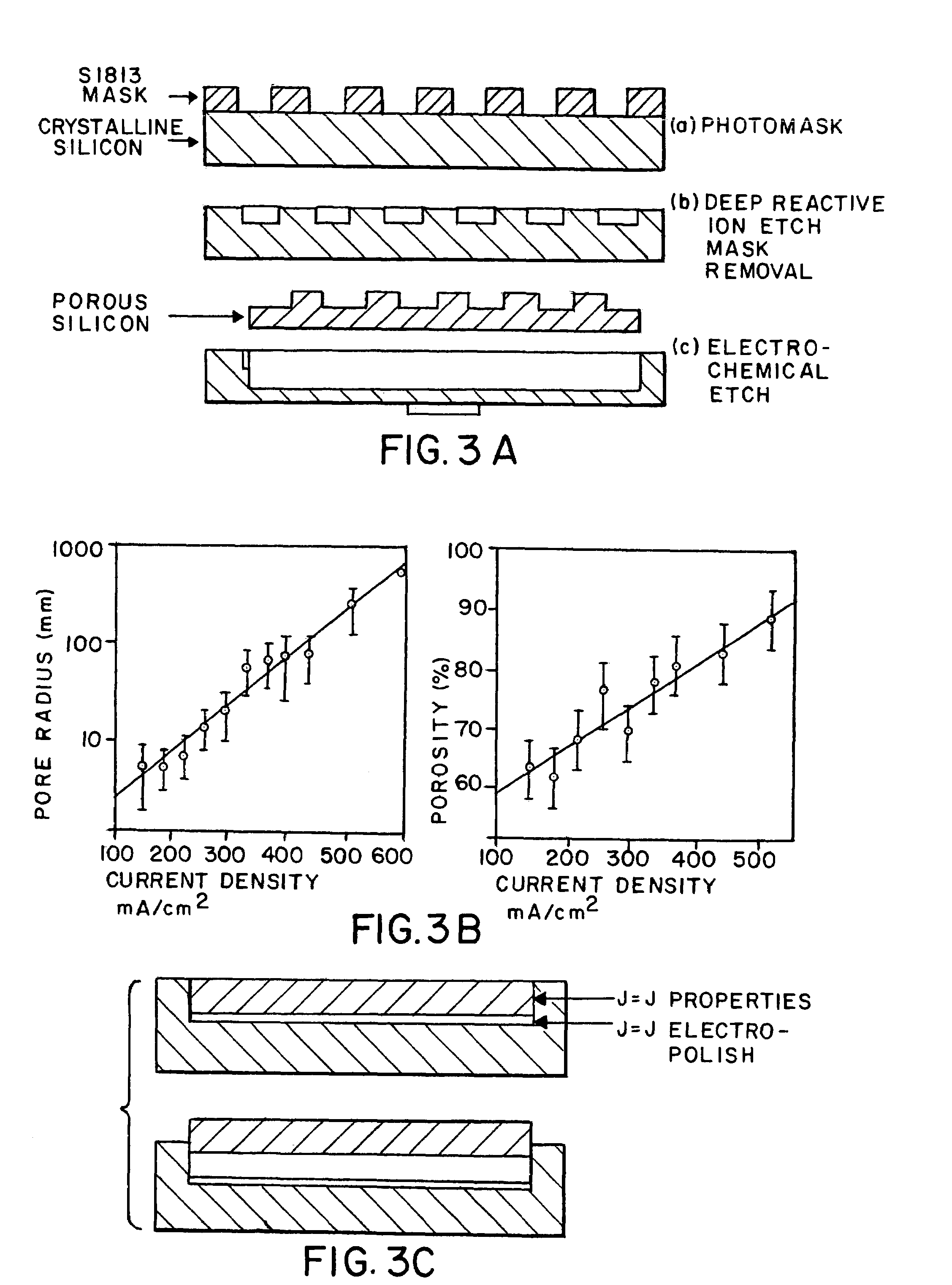
[0045]Photolithography. Silicon wafers were cleaned before application of the positive photoresist. Silicon wafers were cleaned in HCl:MeOH (1:1) and rinsed in deionized water before application of the positive photoresist (Cras et al, 1999). Alternatively, sequential sonication for 5 min. in acetone, isopropanol, and DI water nay be done. The silicon substrates were dried in a 90° C. oven for 90 sec. An approximate 1 micron thick coating of S1813 photoresist was spun onto wafers at 4000 r.p.m. for 25 seconds. The coated chips were then soft baked in a 90° C. oven for 3 min. Masking was performed using a chrome mask and exposing the wafers to UV light of an intensity ˜2 mW / cm2 for 35 sec. The wafer was then placed in 90° C. oven for 6 min. after which it was developed in MF319 developer for 90 sec. The patterned substrate was then placed in a 110° C. oven for 30 min. in order to harden the mask (post-bake). Additionally other etching techniques may be used to stabilize the chips. Th...
example 3
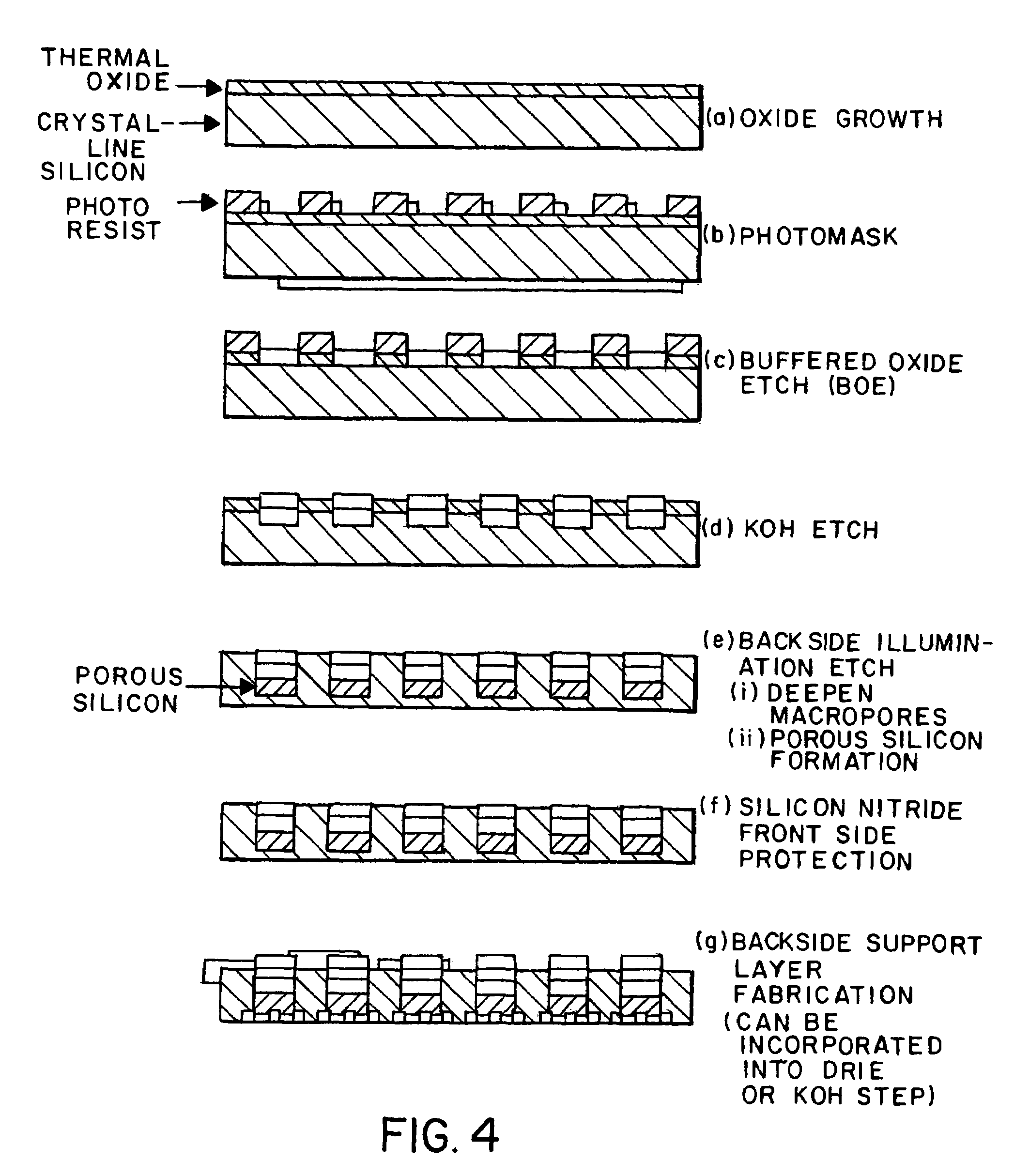
[0046]Methods of fabricating silicon microstructures. Macropores of sizes ranging from 0.5-100 microns may be fabricated using the following three approaches. Methods 1-2 require that further processing as described in Example 4 to created the porous silicon membrane, but in Method 3, the entire chip may be processed in a single step.
[0047]1. Deep reactive ion etch (DRIE) The deep reactive ion etching (DRIE) process is a gas phase technique (dry etch) in which successive passivating / etch steps are performed by exposure to C4F8 and SiF6, respectively. Using the DRIE process, highly anisotropic etches may be created in silicon. A sacrificial oxide layer is not required for this process, unlike the more common wet etch techniques (discussed below). Resist is removed in the DRIE process, however the rate of removal is slow relative to the rate of silicon removal, and thus provided sufficient protection so that the macropores can be produced efficiently. Advantages of the DRIE method inc...
example 4
[0050]Electrochemical Etch. Once the macropores have been formed in the silicon substrate a two-step electrochemical etch in ethanolic HF is performed. There exist numerous variables in the formation of porous silicon however several primary factors have been identified to control pore size and porosity: the type and density of dopant atoms, HF concentration, and current density (J). The methodology that most easily achieves a wide range of variability incorporates highly B-doped silicon (p++-type; r++-type silicon is that the photoconductive effect is much less pronounced than lower doped Si wafers. More exotic applications of the silicon bioreactors are possible with lower doped Si. (Sailor and Lee, 1997)
[0051]In the first step, etching is performed at a current density that provides the desired porosity and pore size. The thickness of the layer is chosen considering the duration of the etch (FIG. 3). In the second lift-off step a current density is chosen near the electropolishin...
PUM
| Property | Measurement | Unit |
|---|---|---|
| diameter | aaaaa | aaaaa |
| diameter | aaaaa | aaaaa |
| diameter | aaaaa | aaaaa |
Abstract
Description
Claims
Application Information


