
Methods for additive repair of phase shift masks by selectively depositing nanometer-scale engineered structures on defective phase shifters

a phase shifter and additive technology, applied in the field of engineering of nanometer-scale structures, can solve the problems of inability to remove hard defects by cleaning process, high cost and complexity of photomasks, and achieve the effect of enhancing the mask

Inactive Publication Date: 2010-04-06
NANOINK INC
View PDF75 Cites 21 Cited by
  • Summary
  • Abstract
  • Description
  • Claims
  • Application Information

AI Technical Summary

Benefits of technology

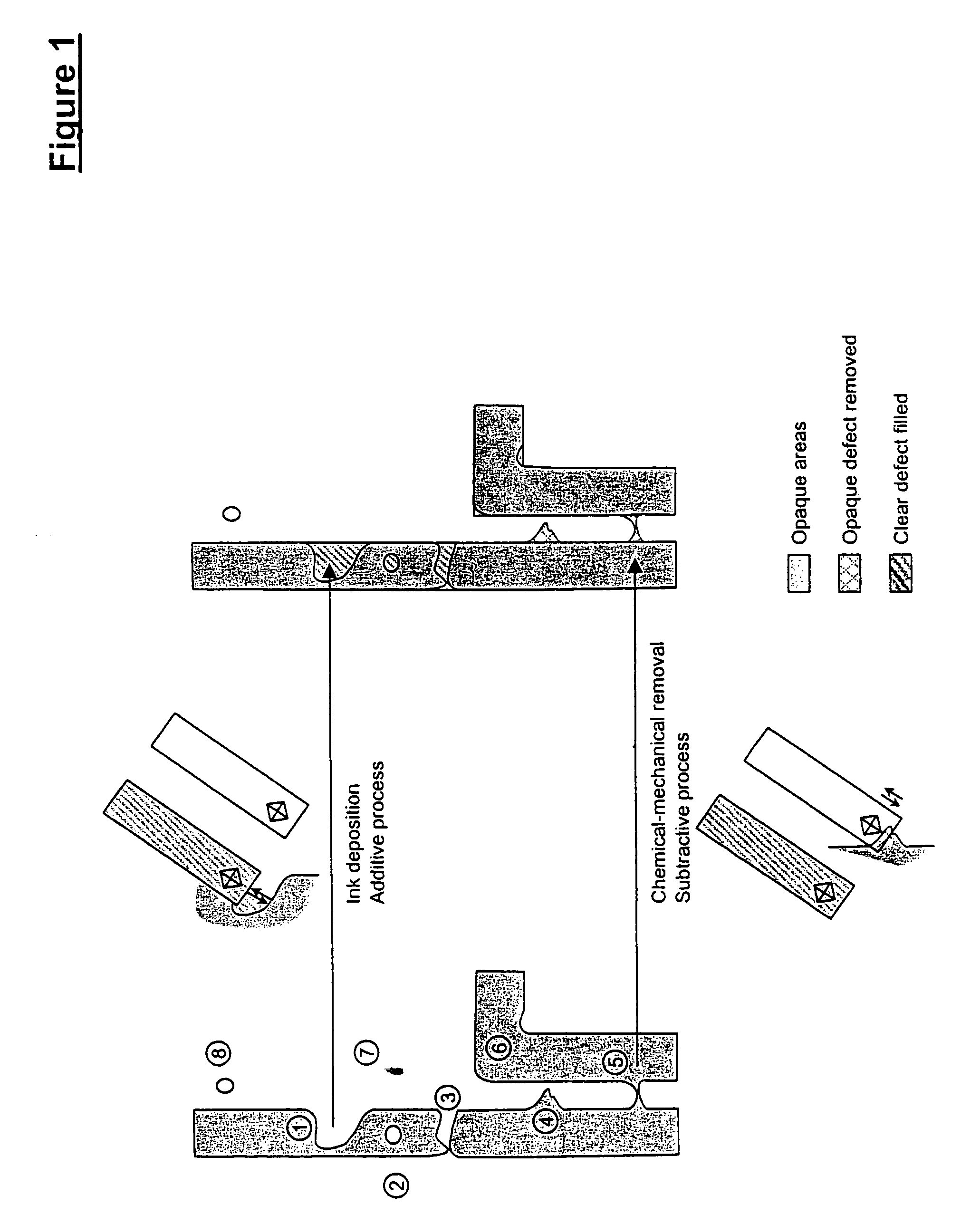
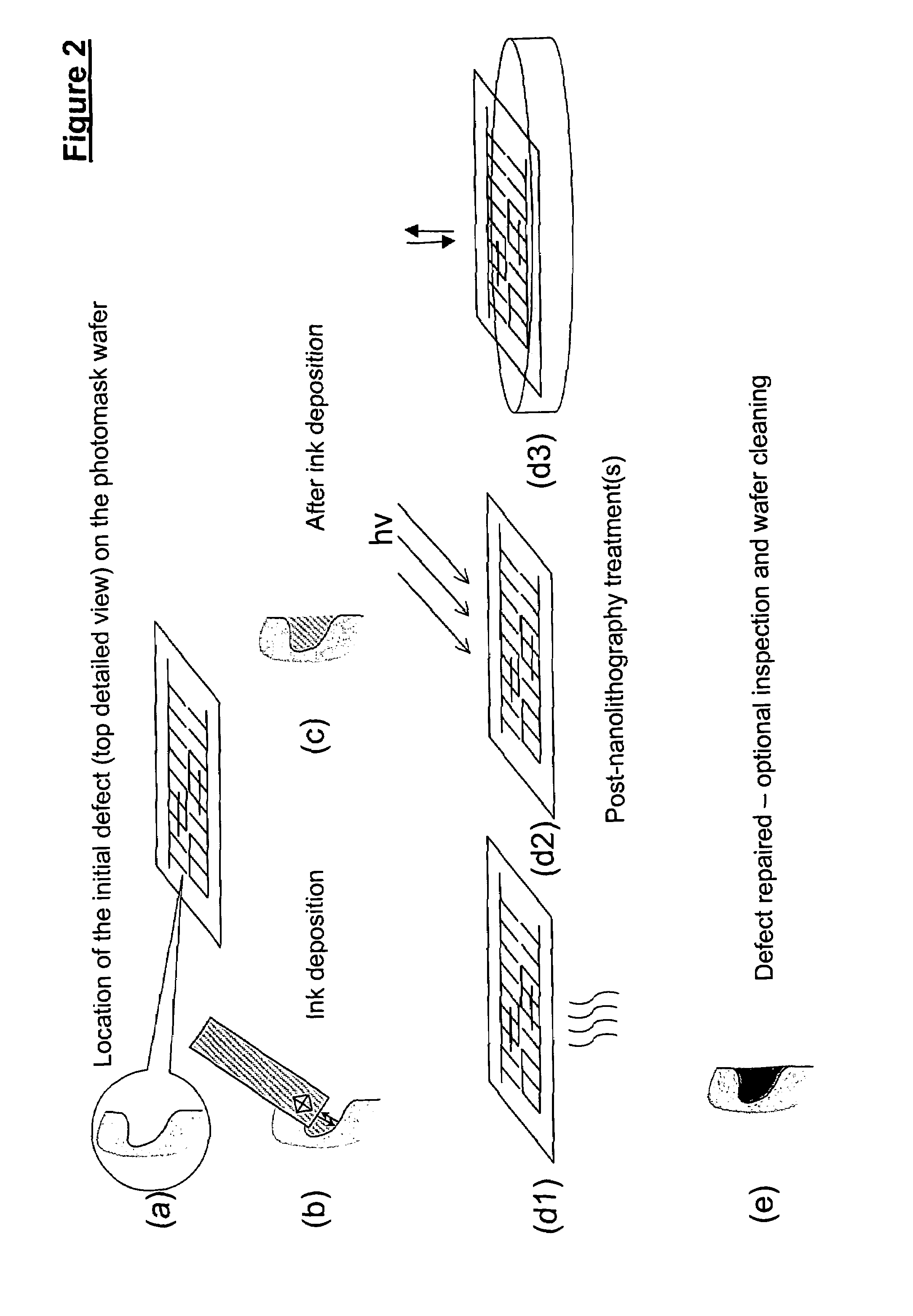
[0010]In the present invention, these and other types of defects can be repaired by improved means of nanolithography and nanodeposition which, among other things, can add material to the mask, or can add materials to and substract materials from the mask. In addition, mask features can be enhanced to include features that may improve performance (e.g., resolution) but are not necessarily patterned or printed. Enhancement features can be, for example, 100 nm structures or less in lateral dimension.
[0015]In addition, even minor defects on the photomasks may result in a global failure of the resulting microchips or may reduce dramatically their mean time before failure. For example, a single extraneous opaque imperfection located between two printed lines on the photomask may result in an electrical short between two electrical paths, triggering a major defect or breakdown of the whole chip. Given the expenses and stringent quality requirements associated with photomasks, it is economically advantageous to (a) repair masks presenting defects after fabrication or after use; (b) modify masks otherwise rendered unusable because of a minor error at design time. It is also important to consider cheaper, more reliable alternatives to current photomask fabrication methods.
[0021]Attenuating PSMs (having weak-shifters) rely on the deposition of a partially transmitting, 180°-phase-shifting material (e.g. molybdenum silicide). Light diffracted from a clear opening in the photomask will destructively interfere with light from the phase-shifted areas, improving contrast. Additive repair of such photomasks relies on the deposition of a layer with similar overall optical properties (transparency, index of refraction), which may be achieved by precise control of the chemistry and the thickness of the patch.
[0041]It is another object of the invention to provide methods (xxvi) to enhance a mask made by conventional methods with features otherwise difficult to fabricate, (xxvii) by addition of OPC (optical proximity correction) features. It is known that image fidelity issues with optical pattern generators limit their usefulness for the patterning of high-density features and sub-resolution OPC features, such as scattering bars. DPN™ patterning with parallel probe arrays may compete effectively with e-beam direct writing, in term of overall costs and throughput, for the fabrication of wavefront engineering features, such as OPC and PSM features.

Problems solved by technology

Typically, photomasks are expensive and complex, and some photomasks contain defects.
A soft defect is typically any defect that can be removed by a cleaning process, whereas a hard defect cannot be removed by a cleaning process.
Other types of defects include those that result from errors in the original mask data tape and also mask misprocessing (misplacement and missizing of geometries; those that result from CD (critical dimension) variations across the masks and edge quality of features, i.e., line edge roughness.
However, photomask feature dimensions are currently approaching their theoretical physical limit.
Photomasks are thus increasingly precise, complex (with the addition of optical phase correction (OPC) and the use of techniques such as phase shifting and off-axis illumination, OAI) and therefore increasingly expensive, for example, typically above $50,000 per unit for alternating phase shift masks.
In addition, even minor defects on the photomasks may result in a global failure of the resulting microchips or may reduce dramatically their mean time before failure.
For example, a single extraneous opaque imperfection located between two printed lines on the photomask may result in an electrical short between two electrical paths, triggering a major defect or breakdown of the whole chip.
Currently used photomask repair processes are either extremely expensive, limited, or not well adapted to advanced mask technologies.
While this technology can work for COG (Chromium on glass), despite poor edge placement accuracy, repair technologies based on gallium staining are known to damage the areas surrounding the defect in attenuating phase shifting masks.
Thus far, additive repair with this tool can only be accomplished by successive deposition of large carbon patches using e.g. focused ion beam (FIB) and then trimming of excess material from the patch.
Light diffracted from a clear opening in the photomask will destructively interfere with light from the phase-shifted areas, improving contrast.
This makes defect inspection and repair absolutely critical.
It is known that image fidelity issues with optical pattern generators limit their usefulness for the patterning of high-density features and sub-resolution OPC features, such as scattering bars.

Method used


Image

  • Methods for additive repair of phase shift masks by selectively depositing nanometer-scale engineered structures on defective phase shifters
  • Methods for additive repair of phase shift masks by selectively depositing nanometer-scale engineered structures on defective phase shifters
  • Methods for additive repair of phase shift masks by selectively depositing nanometer-scale engineered structures on defective phase shifters

Examples


example 1

[0168]A polymer or polymer precursor is deposited and air-dried or air-cured. To obtain optically adequate (i.e. opaque) deposits, the curable polymer / precursor may be mixed with a colloidal solution, esp. metallic or metal oxide nanoparticles. Commercially available inks include water-, methylisobutyl ketone or isopropanol-based silver and carbon nanoparticle paints, such as these commercialized by Ted Pella, Inc.

example 2

[0169]A priming layer, such as ω-functionalized self-assembled monolayer (e.g. trialkoxy- or trichlorosilanes on quartz, alkanethiols on coinage metals) is deposited on the substrate. The ω-terminal functional group (e.g. —SH, —COOH, —CHO . . . ) is selected as a function of the subsequent inks to deposit. For example, ligand-protected metallic colloids (gold, silver) may adhere by place-exchange between the ligand and the layer terminal group, and by electrostatic interaction. In another example, a (e.g., amine-rich or carboxylic acid-rich) polyelectrolyte is deposited that has an opposite charge to that of the ω-terminal group. Charged colloidal particles may then be deposited to form an electrostatic sandwich, as described by Chen et al [K. M. Chen, X. Jiang, L. C. Kimerling and P. T. Hammond, “Selective Self Organization of Colloids on Patterned Polyelectrolyte Templates”, Langmuir, 16, 7825-7834 (2000).] and by Wuelfing et al (Chem. Mater. 2001, 13, 87-95)

Part 2

Deposition and A...

example 3

Metal Deposition and Chemical Reduction

[0171]Palladium chloride (PdCl2) or acetate was deposited from an aqueous solution by DPN™ printing or deposition in the area to fill with metal. The palladium salt structures were reduced to the metallic state, Pd0, by deposition of a reducing agent (e.g. stannous chloride (SnCl2), aqueous dimethylamine-borane, dimethylsulfide:borane, or sodium borohydride) by DPN™ printing or deposition, or flooding, or immersion of the substrate in a bath containing a solution of the reducing agent. This procedure may also be used to deposit other metals, such as silver, copper, iron, platinum, gold, and cobalt when the appropriate metal salt is chosen as an ink.

[0172]FIG. 10. (Working Example) AFM images before and after the reduction reaction are shown in FIG. 10. Deposition of disodium palladium chloride (1 mg / μL in water) with 10% polyethyleneoxide (MW 10,000) via DPN™ printing on amino-silanized glass (Schott Glass company), and subsequent chemical redu...


PUM

PropertyMeasurementUnit
heightaaaaaaaaaa
heightaaaaaaaaaa
heightaaaaaaaaaa

Abstract

Photomask repair and fabrication with use of direct-write nanolithography, including use of scanning probe microscopic tips (e.g., atomic force microscope tips, etc.) for deposition of ink materials including sol-gel inks. Additive methods can be combined with subtractive methods. Holes can be filled with nanostructures. Heights of the nanostructures filling the holes can be controlled without losing control of the lateral dimensions of the nanostructures. Phase shifters on phase shifting masks (PSMs) are additively repaired with selectively deposited sol-gel material that is converted to solid oxide, which has optical transparency and index of refraction adapted for the phase shifters repaired.

Description

RELATED APPLICATIONS[0001]This application claims priority benefit to provisional application 60 / 419,781 filed Oct. 21, 2002 to Crocker et al. (“Nanometer-scale engineered structures, methods and apparatus for fabrication thereof, and applications to photomask repair and enhancement”), which is hereby incorporated by reference in its entirety.INTRODUCTION[0002]The present invention relates in general to the engineering of nanometer-scale structures and, in particular, to the repair and fabrication of masks used for lithography. Applications include the semiconductor industry.[0003]Masks including photomasks are important to the semiconductor industry. Photomask fabrication and repair is an important technology in the semiconductor industry for microchip / integregrated circuit (IC) production by microlithography. See, for example, Handbook of Microlithography, Micromachining, and Microfabrication, Vol. I and II, including Vol. I, Chapter 5 “Photomask Fabrication Procedures and Limitat...

Claims


Application Information

Patent Timeline
Patent Type & Authority Patents(United States)
IPC IPC(8): G03F1/00B05D3/00B32B43/00G03F1/14B82B3/00G03F1/26C23C18/14C23C18/16C23C18/28G01Q30/16G01Q60/00G03F7/00G03F9/00G21K5/00
CPCB82Y10/00C23C18/1612B82Y40/00C23C18/14C23C18/1605C23C18/1658G03F1/72G03F7/0002C23C18/161C09D11/52C23C18/06C23C18/1208C23C18/1254Y10S977/863Y10S977/857B82Y30/00C23C18/143C23C18/145G03F7/00B82B3/00
Inventor CROCKER, PERCY VANCRUCHON-DUPEYRAT, SYLVAINDEMERS, LINETTEELGHANIAN, ROBERTDISAWAL, SANDEEPAMRO, NABILZHANG, HUA
Owner NANOINK INC
Learn More