Electrochemical levelling and polishing processing method with nanometer precision and device thereof

A processing device, electrochemical technology, applied in circuits, electrical components, electrolysis processes, etc., can solve problems such as deep damage layer, surface scratches, metal ion pollution, etc.

Active Publication Date: 2010-11-10
XIAMEN UNIV
View PDF4 Cites 33 Cited by
  • Summary
  • Abstract
  • Description
  • Claims
  • Application Information

AI Technical Summary

Problems solved by technology

However, due to the unevenness of mechanical grinding and external pressure, the surface roughness after polishing is relatively high, which directly affects the processing and yield of subsequent processes.
Since most of the current Al 2 o 3 Abrasive, this type of abrasive has high hardness, large dispersion and high viscosity, so it is easy to cause surface scratches, and the damage layer is deep
In addition, there are problems such as metal ion contamination, poor dispersion, low material removal rate in alkaline environment, etc.
At the same time, the end point detection and control of leveling and polishing is also one of the most difficult problems in the application of CMP technology that can cause the failure of the entire processing process. Excessive polishing or insufficient polishing will cause subsequent processes to fail; more importantly, the future ULSI manufacturing The requirements for surface development have reached nanometer-level surface precision and sub-nanometer surface roughness, which are close to or exceed the limit of surface processing by CMP technology (20mm×20mm, flatness difference <20nm)
In recent years, CMP technology uses electrochemistry as an auxiliary means to improve the surface leveling and polishing effect of conductive metal copper or other semiconductor materials by means of electrochemical anodic dissolution. However, the inherent shortcomings of the above-mentioned CMP technology have not been eliminated.

Method used


Image

  • Electrochemical levelling and polishing processing method with nanometer precision and device thereof
  • Electrochemical levelling and polishing processing method with nanometer precision and device thereof
  • Electrochemical levelling and polishing processing method with nanometer precision and device thereof

Examples


Embodiment 1

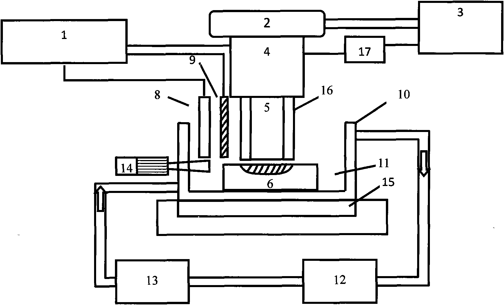
[0058] Example 1: figure 1 A composition schematic diagram of an implementation device example of the leveling and polishing processing method of the present invention is given. The processing tool adopts a platinum disc-shaped tool 5 with nano-flat precision on the surface. The tool 5 is fixed on the lower part of the metal holder 4, and the fiber optic probe 16 of the parallel laser beam distance measuring device 17 fixed on the outside of the tool is also fixed on the metal holder. The bottom of 4, parallel laser beam ranging device 17 links to each other with information processing computer 3, and metal fixed frame 4 can adopt two sections of cylinders with different diameters, and its top connects the Z-axis (vertical axis) micro-drive controller 2 of drive unit, The Z-axis micro-driver 2 is connected to the information processing computer 3; the electrochemical system is provided with a potentiostat 1, an auxiliary electrode 8, a reference electrode 9, a container 10, a ...

Embodiment 2

[0062] Example 2: Figure 6 A microscopic image of the silicon surface of Example 2 of polishing on the silicon surface according to the present invention is given. Processing conditions: the circulating solution contains 0.1mol / dm 3 Ammonium Fluoride (NH 4 F), 1mmol / dm 3 Tetramethylammonium bromide ((CH 4 ) 4 NBr), 0.01mol / dm 3 L-cystine (L-cystine) and 0.5mol / dm 3 Sulfuric acid (H 2 SO 4 ); its temperature is maintained at 30°C during the entire etching and leveling process; after the electrochemical etching reaction control system is started, bromide ions (Br - ) produces bromine (Br 2 ) etch leveling agent; the scavenger is cystine (L-cystine); in the whole leveling and polishing process, the electrode potential of the tool (metal platinum disk electrode) is kept at 0.9V (relative to the saturation potential of the calomel electrode). Among them, the surface of the platinum metal disk is polished by CMP technology, and its flatness accuracy is greater than 60nm,...

Embodiment 3

[0063] Example 3: Figure 7 A microscopic image of the copper surface of Example 3 of the inventive polishing on the copper surface is given. Processing conditions: the circulating solution contains 0.1mol / dm 3 Acetic acid (pH 5.5), 2mg dm -3 Benzotriazole, 10mmol / dm 3 Sodium thiosulfate (Na 2 S 2 o 8 ) and 0.1mol / dm 3 N-acetylcysteine; its temperature is maintained at 30°C throughout the etching and leveling process; after the electrochemical etching reaction control system is started, Na is electrolyzed on the surface of the platinum metal disk 2 S 2 o 8 produce Free radical etching leveling agent; the scavenger is N-acetylcysteine ​​added to the etching solution; the electrode potential of the tool (metal platinum disk electrode) is maintained at -0.5 during the entire leveling and polishing process by a constant potential method V (potential relative to saturated calomel electrode). Among them, the surface of the platinum metal disk is polished by CMP technolog...


PUM


Abstract

The invention provides an electrochemical levelling and polishing processing method with nanometer precision and a device thereof, relating to an electrochemical etching levelling and polishing technology. The device is provided with a cutter with nanometer levelling precision, an electrochemical reaction control system capable of accurately controlling the thickness of an etching levelling agent liquid layer in nanoscale, a solution circulating device, a solution thermostat and an automatic control system. The method is implemented by the following steps: preparing the cutter with nanometer levelling precision to serve as an electrochemical working electrode, and placing the cutter at the bottom of a container together with a workpiece; immersing the cutter in a solution, starting an electrochemical system, generating the etching levelling agent on the surface of the cutter, compressing the etching levelling agent liquid layer on the cutter surface into a nanoscale thickness, and regulating and controlling the thickness of the etching levelling agent liquid layer; driving a tri-dimensional micro-drive device, leading the cutter to approach the workpiece gradually, and regulating and controlling the distance and parallelism between the workpiece surface and the cutter; and leading the cutter to move toward the workpiece surface, and enabling the constraint etching levelling agent liquid layer on the cuter surface to contact with the workpiece surface until the whole workpiece is etched, leveled and polished.

Description

technical field [0001] The invention relates to an electrochemical etching leveling and polishing technology, in particular to a large-area and batch electrochemical etching leveling and polishing processing method and device for performing nanometer leveling precision on the surfaces of metals, semiconductors and insulators. Background technique [0002] Semiconductor ultra-large-scale integrated circuit (ULSI) manufacturing technology has developed to the era of 120nm characteristic linewidth and 300mm diameter wafer, and the technology with characteristic linewidth of 100nm is also entering the market. Today, the number of transistors on a single chip has exceeded 100 million. According to According to the blueprint for the development of microelectronics technology by the American Semiconductor Industry Association, the characteristic line width will be reduced to 50nm by 2011, and 450mm wafers will be used at that time, and the number of metal layers will move from 5 to ...

Claims


Application Information

Patent Timeline
Patent Type & Authority Applications(China)
IPC IPC(8): C25F3/12H01L21/3063
CPCC25F3/12H01L21/02024C25F3/14C25F3/00H01L21/30604H01L21/7684H01L21/32115C25F7/00H01L21/30612H01L21/3063C03C15/02
Inventor 田中群时康詹东平田昭武韩联欢汤儆
Owner XIAMEN UNIV
Why Eureka
Try Eureka