Coupled optical and optoelectronic devices, and method of making the same

a technology of optical and optoelectronic devices and coupling devices, which is applied in the direction of optical waveguide light guides, optical elements, instruments, etc., can solve the problems of spherical lens chromatic aberration, and no other approach can compare with the high device densities and high yield, so as to achieve the effect of being easily manufactured and not sacrificing speed and power performan

Inactive Publication Date: 2005-03-22
PSEMI CORP
View PDF35 Cites 50 Cited by
  • Summary
  • Abstract
  • Description
  • Claims
  • Application Information

AI Technical Summary

Benefits of technology

The present invention describes devices (and methods for making such devices) that provide optical-optoelectronic coupling and that overcome many of the disadvantages and shortcomings of previously described devices and me...

Problems solved by technology

Applications that require manipulation of many optical signals are becoming more complex and more commonplace.
No other approach can compare with the high device densities and high yields available with silicon CMOS technology.
At the size of an optical fiber, spherical aberration and chromatic aberration of spherical lenses are very disadvantageous.
Because the fiber mounting blocks are relatively thin, i.e. in the range of about 30 mils thick, the requirements of the electrical connection and the orthogonally mounted optoelectronic chip lead to a height mismatch and the need for a supporting member, which leads to added size, and with the wire bonds, added failure modes.
The manufacturability of such optical/optoelectronic integrated modules is challenging, however, because of the need to etch very different profiles into the same silicon substrate, requiring many masking/demasking steps.
Various methods have been tried, with less than ideal results.
Heteroepitaxial growth of GaAs on silicon, and silicon on GaAs have been explored, but after decades of research, fundamental problems such as the mismatch in the crystal lattice constants, cross-contamination, incompatibilities of device processing, and the diff...

Method used


Image

  • Coupled optical and optoelectronic devices, and method of making the same
  • Coupled optical and optoelectronic devices, and method of making the same
  • Coupled optical and optoelectronic devices, and method of making the same

Examples


Embodiment Construction

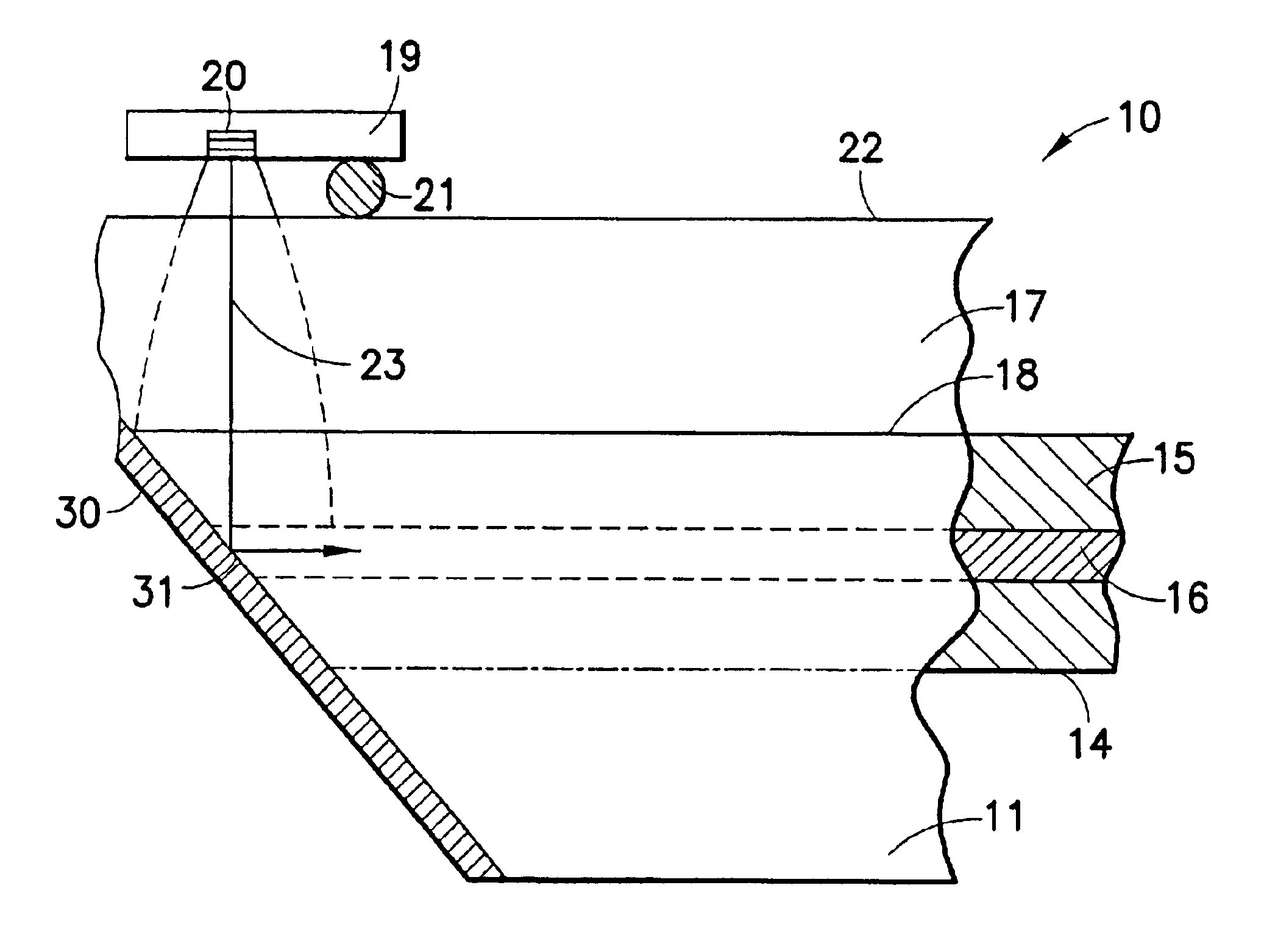
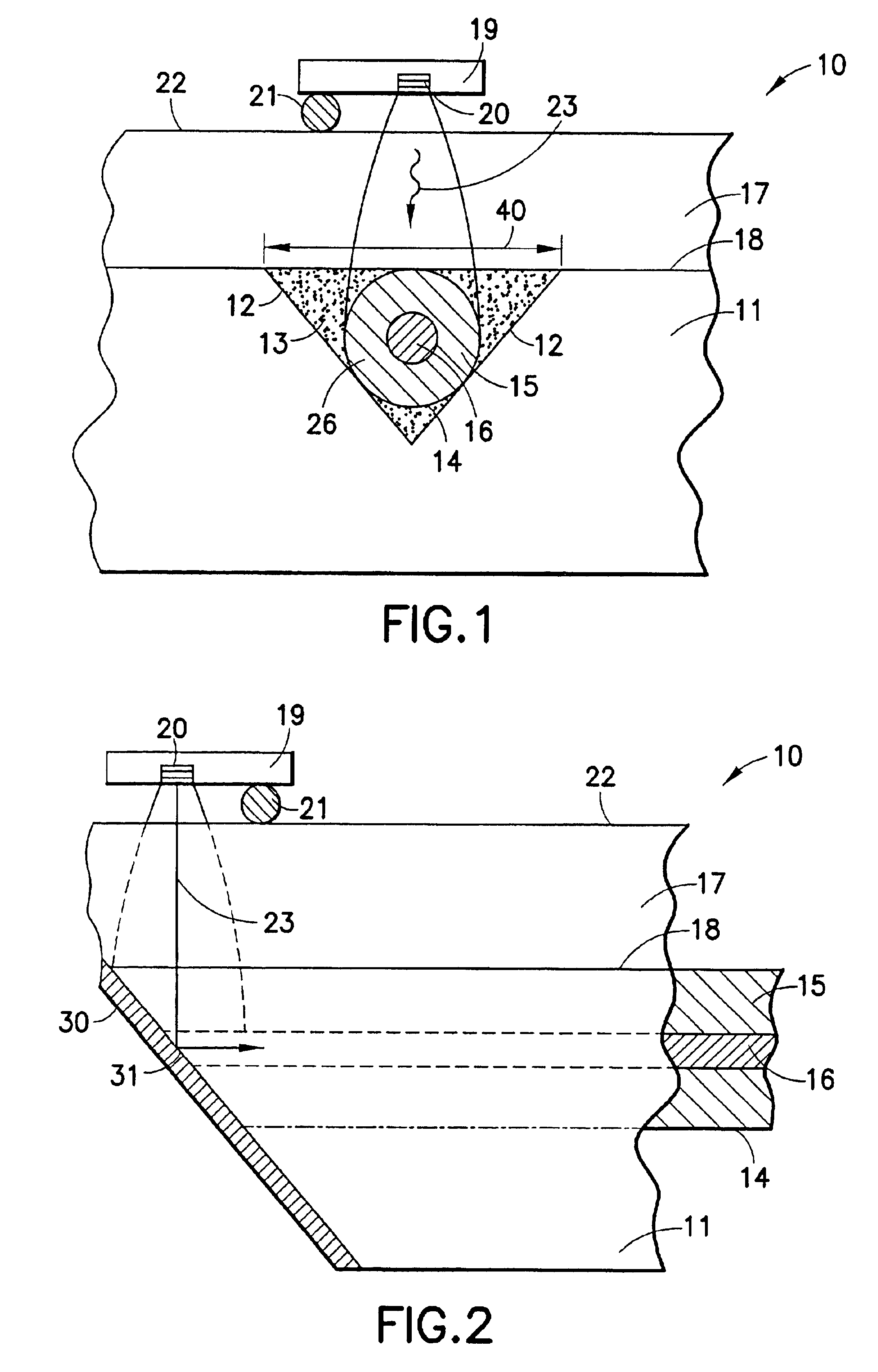
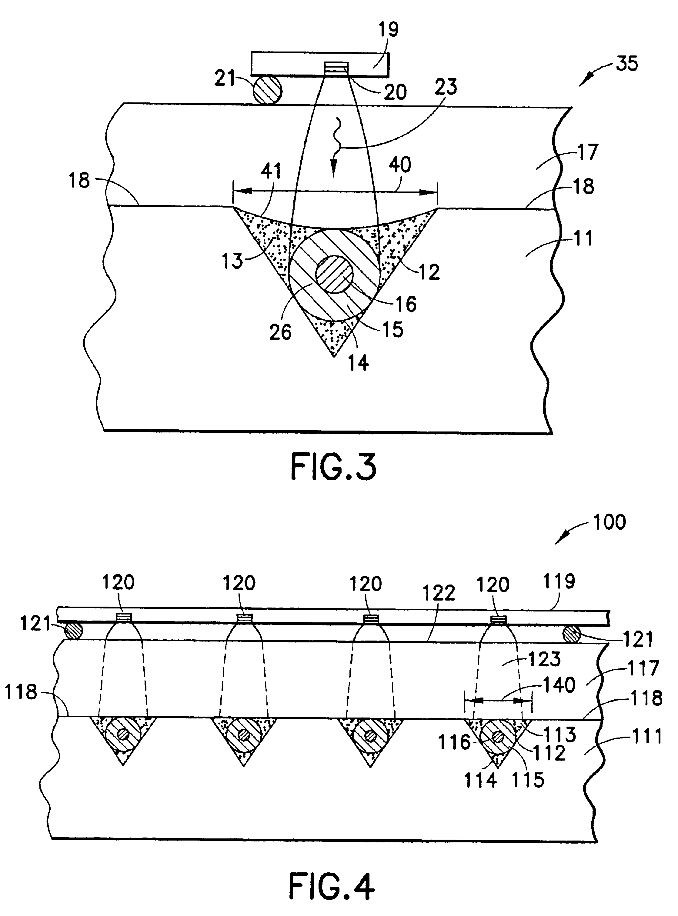
Integration of silicon and optoelectronic devices on a common insulating transparent substrate requires that an effective method for forming silicon CMOS devices on the transparent, insulating substrate be used. It has been found that high quality silicon films suitable for demanding device applications can be fabricated on sapphire substrates by a method that involves epitaxial deposition of a silicon layer on a sapphire substrate, low temperature ion implant to form a buried amorphous region in the silicon layer, and annealing the composite at temperatures below about 950° C.

Examples of and methods for making such silicon-on-sapphire devices are described in U.S. Pat. No. 5,416,043 (“Minimum charge FET fabricated on an ultrathin silicon on sapphire wafer”); U.S. Pat. No. 5,492,857 (“High-frequency wireless communication system on a single ultrathin silicon on sapphire chip”); U.S. Pat. No. 5,572,040 (“High-frequency wireless communication system on a single ultrathin silicon on sa...


PUM


Abstract

An optical-optoelectronic coupling structure comprising a flip-chip optoelectronic/ultrathin silicon-on-sapphire device mounted on a V-groove, optical-fiber-bearing carrier substrate, including light-reflective structures for launching light into the optical fiber core or transmitting light emitted by the optical fiber core to the optoelectronic device. The optical fiber may be immobilized in the V-groove using a curable resin adhesive characterized by a refractive index substantially similar to the refractive index of the optical fiber.

Description

FIELD OF THE INVENTIONThe present invention relates to a method and apparatus for coupling light between optical fibers and optoelectronic devices for optical signal processing. Optical / optoelectronic coupling structures of the invention may variously include light receivers, transmitters, and transceivers.BACKGROUND OF THE INVENTIONApplications that require manipulation of many optical signals are becoming more complex and more commonplace. Such applications include the routing of signals in fiber optic networks, necessitated by, for example, telecommunications and large volumes of internet traffic. In fiber optic networks, large volumes of optical signals must be transmitted between optical fibers and optoelectronic devices; optical signals must be processed and retransmitted as electrical or optical signals; electrical signals must be processed and transmitted as optical signals. The optical fibers are typically present as arrays of up to 100×100 fibers; larger arrays are possibl...

Claims


Application Information

Patent Timeline
IPC IPC(8): G02B6/42
CPCG02B6/4214G02B6/4249G02B6/4231G02B6/4204G02B6/4212G02B6/4239G02B6/4246G02B6/4259G02B6/4274G02B6/4267G02B6/426G02B6/4243G02B6/4261H01L2224/16H01L2924/13091H01L2924/00
Inventor REEDY, RONALD E.CABLE, JAMES S.KUZNIA, CHARLES B.ALBARES, DONALD J.LE, TRI Q.
Owner PSEMI CORP
Why Eureka
Try Eureka