
Fluidic nanotubes and devices

a technology of fluidic nanotubes and nanotubes, which is applied in the field of fluidic devices, can solve the problems of general hydrophobicity of nanotubes and may not be suitable for fluidic applications without modification, and achieve the effects of reducing the size, weight and cost of sensors and sensor arrays, and increasing spatial and temporal resolution and accuracy

Inactive Publication Date: 2008-04-08
RGT UNIV OF CALIFORNIA
View PDF8 Cites 72 Cited by
  • Summary
  • Abstract
  • Description
  • Claims
  • Application Information

AI Technical Summary

Benefits of technology

[0029]The present invention pertains to fluidic nanotubes and devices fabricated from fluidic nanotubes. The fabrication of oriented, robust nanotube arrays is of interest for their potential use in nanoscale fluidic bioseparation, sensing, catalysis, and so forth. Sensors utilizing novel nanostructured materials and new mechanisms may significantly benefit a broad range of applications relating to national security, health care, the environment, energy, food safety, and manufacturing. Emerging micro- and nano-technologies can decrease the size, weight and cost of sensors and sensor arrays by orders of magnitude, and increase their spatial and temporal resolution and accuracy.
[0030]Over the years, various molecular detection techniques have been developed and validated for their chemical / biological sensing, diagnostic and prognostic utility. For most, efficiency is a result of a trade-off between sensitivity, specificity, ease of operation, cost, speed and few false alarms. Novel functional materials such as quantum dots, photonic crystals, nanowires, carbon nanotubes, porous membranes, porous silicon and sol-gel matrices incorporating biomolecules have been used as sensing elements with various possible detection mechanisms. In addition, the growth of nanotubes would be advantageous in potential nanoscale electronics, optoelectronics, and biochemical sensing applications.
[0038]In one embodiment, NEAT / TFET is based on the use of nanocapillaries 5-20 nm in diameter and made of silicon dioxide (SiO2) or semiconductor gallium nitride (GaN). The inner surface of these nanocapillaries will be functionalized by probe / receptor ligands. A mixture of biomolecules in an ionic solution will be electrophoretically transported through the nanocapillary while the ionic current or the conductivity of the semiconductor tube is monitored. If a target ligand specifically binds to the probe molecules attached to the wall, the residence time of the ligand inside the nanocapillary will be much longer than that for non-binding molecules passing through it. Because the nanocapillaries are on the order of molecular size (5-20 nm diameter), the ionic current will be modulated by the presence or absence of specifically-bound ligands as well as the molecule size. In addition, if there is any charge transfer between the analytes and the semiconductor GaN nanotubes, the conductivity of the tubes can be modified and monitored accordingly. Multiple electrical signals (ionic current and source-drain current) and optical signatures can be used simultaneously for the sensing purposes. In addition, parallel processing and integration of nanocapillary arrays can be used for fabrication of nanofluidic chips for multiplexed chemical and biological sensing. The invention facilitates chemical and biological sensors with fast response, ultrasensitivity, high specificity and few false alarms.
[0044]The electrical sensing of movement through the electrophoresis device can be augmented with conventional sensing for reducing false positives. One embodiment therefore includes: (a) an optical single-molecule detection and identification system configured for generating an optical detection signal in response to molecules passing through the nanotube; and (b) a coincidence circuit configured to generate coincident molecule detection signals in response to the coincidence between the ionic current flow and the optical detection signal.
[0067]Another aspect of the invention is to provide a common sensing platform for health, environment and battlefield applications, while emphasizing high sensitivity, high specificity, cost effectiveness, and user friendliness.

Problems solved by technology

While fluidic devices can be made using carbon-based nanotubes, such nanotubes are generally hydrophobic and may be unsuitable for fluidic applications without modification.

Method used


Image

  • Fluidic nanotubes and devices
  • Fluidic nanotubes and devices
  • Fluidic nanotubes and devices

Examples


example 1

[0129]The nanowire cores employed in the present invention can be formed in any conventional manner. For example, arrays of zinc oxide (ZnO) nanowires were grown on a substrate material, such as (110) sapphire wafers, preferably using a vapor deposition process. These ZnO nanowire arrays were placed inside a reaction tube (i.e. MOCVD reaction tube) for GaN chemical vapor deposition. Trimethylgallium and ammonia were used as precursors and fed into the system with argon or nitrogen carrier gas. The deposition temperature was preferably set at 600° C. to 700° C.

[0130]After the GaN deposition, the samples were treated in a hydrogen atmosphere at elevated temperature, such as 600° C. with 10% H2 in argon, for removing the ZnO nanowire templates. It should be appreciated that other methods and materials may be utilized (although in some instances less preferably) for forming the nanowires, covering the nanowires with the nanotube material, and for sacrificially removing the nanowire mate...

example 2

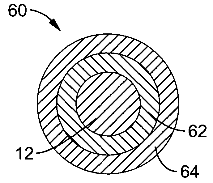
[0153]FIG. 18A illustrates silicon nanowire arrays which were prepared using chemical vapor deposition (CVD) epitaxial growth employing silicon tetrachloride (SiCl4, Aldrich, 99.99%) as the silicon source. Hydrogen (10% balanced by argon) was used to reduce SiCl4 at high temperature (900-950° C.). Gold (Au) thin film was coated on Si (111) substrates 30 to initiate the growth of silicon nanowires 32 via the vapor-liquid-solid growth mechanism. The gold remains as caps 34 on the Si nanowires. This approach to growing Si nanowires was developed and is utilized by the inventors for the synthesis of vertical Si / SiGe superlattice nanowire arrays. The silicon nanowire array samples were heated, such as loaded into a tube furnace and heated at 800-1000° C. for one hour under the continuous flow of pure oxygen (O2).

[0154]FIG. 18B depicts the nanowires 32 after being uniformly oxidized to provide SiO2 sheaths 36 with continuous silicon cores inside. During oxidation, the nanowire tips 34 are...

example 3

[0161]FIG. 19A-19D are images of nanotube formation according to the invention, registered as scanning electron micrographs (SEM). A silicon nanowire array is shown in FIG. 19A, with the Si nanowires vertically orientated to form a substantially perfect array. Typical sizes of the silicon nanowires are 50-200 nm, and the length is around 8 μm. On the top of each nanowire can be seen a bright gold tip indicative of the vapor-liquid-solid growth.

[0162]FIG. 19B illustrates the nanotubes after parylene deposition, SiO2 cap removal, and the etching of the silicon cores, wherein a silica nanotube array embedded in parylene membrane is formed. The pores can be readily seen on the polymer surface. The bright spots on the image corresponding to the gold nanoparticle tips, which nearly take the shape of half spheres. The membrane has a relatively flat surface. The inset within FIG. 19B depicts high magnification of two silica nanotubes embedded in the parylene membrane, clearly showing the ho...


PUM


Abstract

Fluidic nanotube devices are described in which a hydrophilic, non-carbon nanotube, has its ends fluidly coupled to reservoirs. Source and drain contacts are connected to opposing ends of the nanotube, or within each reservoir near the opening of the nanotube. The passage of molecular species can be sensed by measuring current flow (source-drain, ionic, or combination). The tube interior can be functionalized by joining binding molecules so that different molecular species can be sensed by detecting current changes. The nanotube may be a semiconductor, wherein a tubular transistor is formed. A gate electrode can be attached between source and drain to control current flow and ionic flow. By way of example an electrophoretic array embodiment is described, integrating MEMs switches. A variety of applications are described, such as: nanopores, nanocapillary devices, nanoelectrophoretic, DNA sequence detectors, immunosensors, thermoelectric devices, photonic devices, nanoscale fluidic bioseparators, imaging devices, and so forth.

Description

CROSS-REFERENCE TO RELATED APPLICATIONS[0001]This application is a continuation-in-part of U.S. application Ser. No. 10 / 731,745 filed on Dec. 8, 2003 now U.S. Pat. No. 7,211,143, incorporated herein by reference in its entirety, which claims priority to U.S. provisional application Ser. No. 60 / 461,346 filed on Apr. 8, 2003, incorporated herein by reference in its entirety, U.S. provisional application Ser. No. 60 / 454,038 filed on Mar. 11, 2003, incorporated herein by reference in its entirety, and U.S. provisional application Ser. No. 60 / 432,104 filed on Dec. 9, 2002, incorporated herein by reference in its entirety.[0002]This application also claims priority to U.S. provisional application Ser. No. 60 / 461,346 filed on Apr. 8, 2003, incorporated herein by reference in its entirety.STATEMENT REGARDING FEDERALLY SPONSORED RESEARCH OR DEVELOPMENT[0003]This invention was made with Government support under Contract No. DE-AC03-76SF00098, awarded by the Department of Energy and Grant No. ...

Claims


Application Information

Patent Timeline
IPC IPC(8): C30B23/00C30B25/02C30B29/60C30B33/00H01L21/00H01L21/205H01L31/109
CPCB82Y10/00B82Y30/00C30B25/02C30B29/602C30B29/605C30B33/00H01L29/0676H01L29/068H01L21/0242H01L21/02472H01L21/02516H01L21/02521H01L21/0254H01L21/0262H01L21/02639H01L21/02664B01L3/502761G01N27/00B01L2200/0631B01L2200/0663B01L2300/12B01L2300/161
Inventor YANG, PEIDONGHE, RONGRUIGOLDBERGER, JOSHUAFAN, RONGWU, YIYINGLI, DEYUMAJUMDAR, ARUN
Owner RGT UNIV OF CALIFORNIA
Learn More