

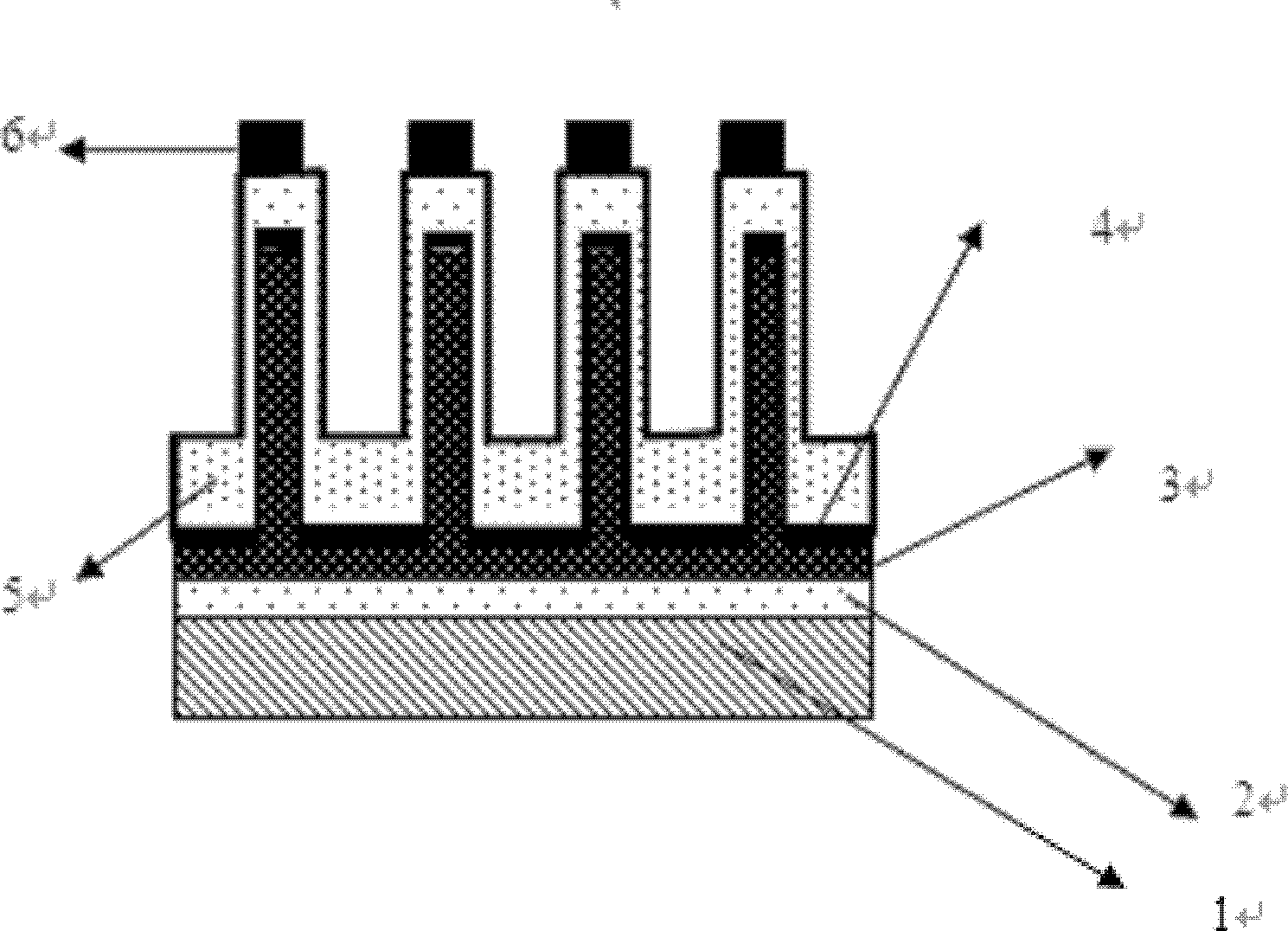
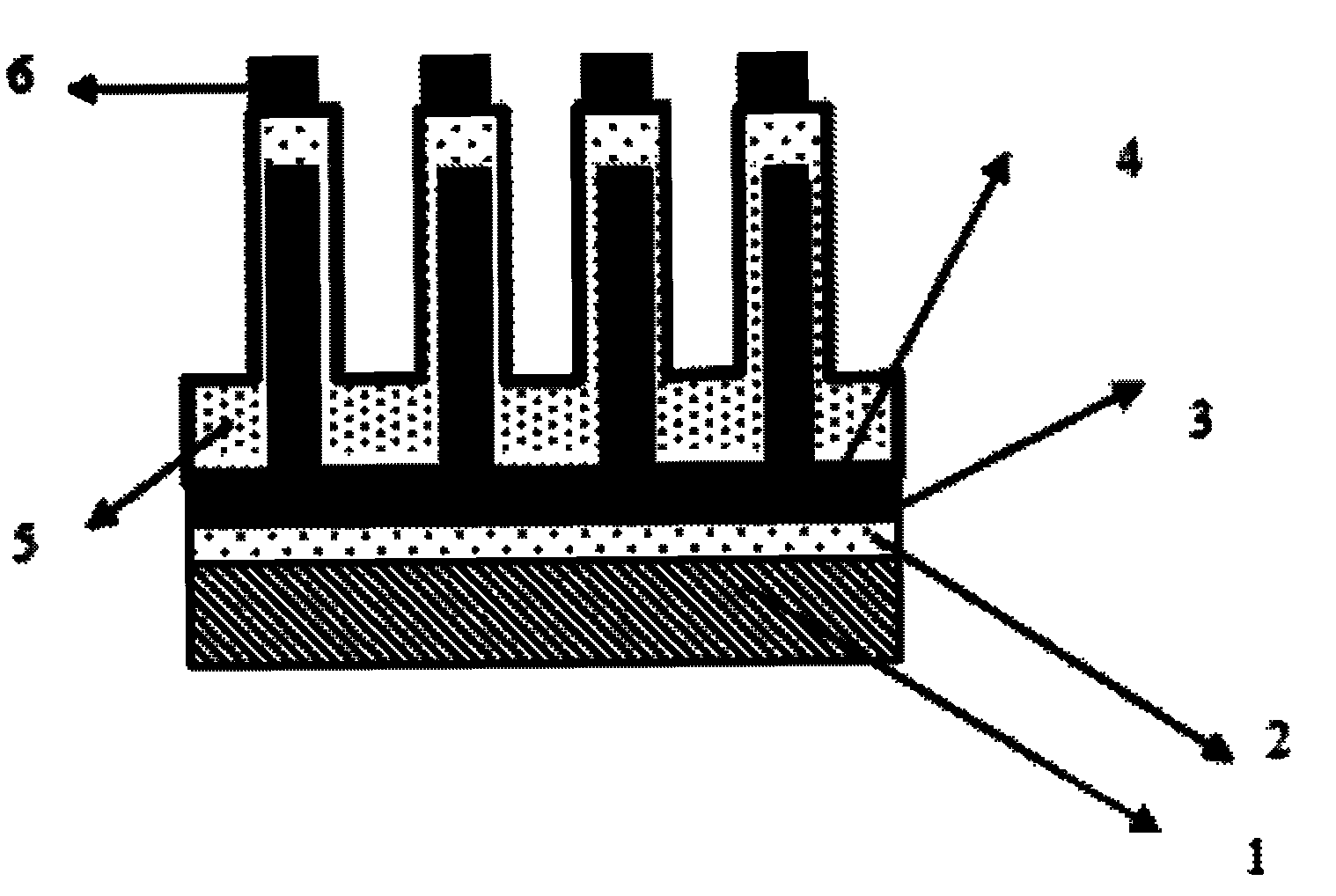
CIGS nanostructure thin-film photovoltaic battery and preparation method thereof
A technology of thin-film photovoltaic cells and nanostructures, which is applied in the manufacture of circuits, electrical components, and final products. It can solve the problems of film crystallinity, easy introduction of impurities, and low production costs. It achieves uniform distribution, low equipment requirements, and low cost effect
- Summary
- Abstract
- Description
- Claims
- Application Information
AI Technical Summary
Problems solved by technology
Method used
Image

Examples
Embodiment 1
[0042] A CIGS nanostructure thin film photovoltaic cell is prepared by the following steps:
[0043] (1) Polish the copper sheet with No. 0-6 sandpaper, and ultrasonically clean it with alcohol, acetone, and deionized water for 5 minutes; then deposit (magnetron sputtering) a layer of Mo on the copper sheet, and the thickness of Mo is 800nm;
[0044] (2) sputtering a layer of copper film with a thickness of 1um on the copper sheet deposited with the Mo layer;
[0045] (3) Mix the product of step (2) with hydrogen sulfide / oxygen mixed gas (the volume ratio of the two is 1:2), and heat at 20°C for 16h to generate copper sulfide nanowires;
[0046] (4) putting the copper sulfide nanowire into 1mol / L dilute hydrochloric acid to dissolve the surface oxide layer;
[0047] (5) The product of step (4) is used as the working electrode, the platinum wire is used as the counter electrode, the reference electrode is selected from SCE, and the acidic solution containing indium chloride is...
Embodiment 2
[0054] A CIGS nanostructure thin film photovoltaic cell is prepared by the following steps:
[0055] (1) The glass sheet is ultrasonically cleaned with 1mol / L NaOH, 1mol / L HCl solution, absolute ethanol, and deionized water in sequence, and then thermally evaporates a layer of Mo on the glass sheet, and the thickness of Mo is 800nm;
[0056] (2) Thermal evaporation of a layer of copper film with a thickness of 1um on the substrate after thermal evaporation of Mo;
[0057] (3) Mix the product of step (2) with hydrogen sulfide / oxygen mixed gas (the volume ratio of the two is 1:2), and heat at 10° C. for 18 hours to grow cuprous sulfide nanowires;
[0058] (4) putting the cuprous sulfide nanowire into 1mol / L dilute hydrochloric acid to dissolve the surface oxide layer;
[0059] (5) the product of step (4) is carried out chemical bath in the mixed solution of ammonium chloride, cadmium chloride, ammoniacal liquor and thiourea, deposits cadmium sulfide shell layer, and thickness i...
Embodiment 3
[0065] A CIGS nanostructure thin film photovoltaic cell is prepared by the following steps:
[0066] (1) The silicon wafer is ultrasonically cleaned with 1mol / L NaOH, 1mol / L HCl solution, absolute ethanol, and deionized water in sequence; then deposit (magnetron sputtering) a layer of Mo on the silicon wafer, the thickness of Mo 800nm;
[0067] (2) sputtering a layer of copper film with a thickness of 1um on the substrate after depositing Mo;
[0068] (3) Mix the product of step (2) with hydrogen sulfide / oxygen mixed gas (the volume ratio of the two is 1:2), and heat at 18° C. for 12 hours to grow cuprous sulfide nanowires;
[0069] (4) putting the cuprous sulfide nanowire into 1mol / L dilute hydrochloric acid to dissolve the surface oxide layer;
[0070] (5) the product of step (4) is used as a working electrode, the counter electrode is a platinum wire, and the working electrode is SCE, and the acidic solution containing indium chloride, gallium chloride and selenous acid i...
PUM
| Property | Measurement | Unit |
|---|---|---|
| thickness | aaaaa | aaaaa |
| thickness | aaaaa | aaaaa |
| thickness | aaaaa | aaaaa |
Abstract
Description
Claims
Application Information