Method for forming thin film
A thin film manufacturing method and thin film technology, which are applied in the field of thin film manufacturing, can solve problems such as aluminum and other metal corrosion, film quality degradation, and the problem of step coverage
- Summary
- Abstract
- Description
- Claims
- Application Information
AI Technical Summary
Problems solved by technology
Method used
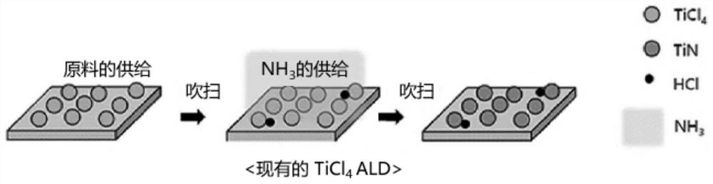
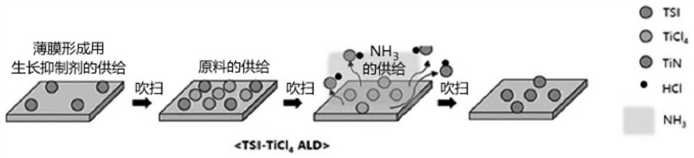
Image

Examples
Embodiment 1 to 7
[0108] Prepare the growth inhibitor for thin film formation and TiCl as the film precursor described in Table 1 below, respectively. 4 . The prepared growth inhibitor for thin film formation was filled in a tank, and supplied to a vaporizer heated to 150° C. at a flow rate of 0.05 g / min using a LMFC (Liquid Mass Flow Controller) at room temperature. After 3 seconds of injecting the growth inhibitor for thin film formation vaporized into the vapor phase in the evaporator into the deposition chamber loaded with the substrate, argon gas was supplied at 3000 sccm for 6 seconds and purged with argon gas. At this time, the pressure in the reaction chamber was controlled to 1.3 Torr. Then, the prepared TiCl 4 It was placed in another tank, and was supplied to another vaporizer heated to 150° C. at a flow rate of 0.05 g / min using LMFC (Liquid Mass Flow Controller) at normal temperature. TiCl vaporized into the vapor phase in the evaporator 4 After being put into the deposition cha...
experiment example
[0116] 1) Deposition evaluation
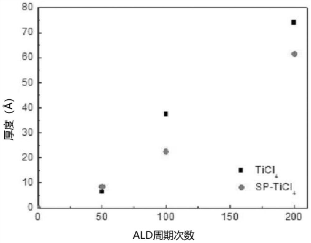
[0117] Referring to Table 2 below, Example 1 in which 2-chloro-2-methylbutane was used as a growth inhibitor for film formation was compared with Comparative Example 1 in which it was not included. As a result, the deposition rate is Compared with Comparative Example 1, the deposition rate was reduced by more than 55.5%. It could be confirmed that the remaining Examples 2 to 7 also had similar deposition rates as Example 1. In addition, it was confirmed that Comparative Examples 2 and 3, which did not use the growth inhibitor for thin film formation of the present invention but used pentane or cyclopentane, also had the same deposition rate as Comparative Example 1. At this time, a decrease in the deposition rate indicates a change in CVD deposition characteristics to ALD deposition characteristics, and thus can be used as an index of improvement in step coverage characteristics.
[0118] Table 2
[0119]
[0120] In addition, as sho...
Embodiment 1
[0136] In addition to using Tris(dimethylamino)cyclopentadienylzirconium (Tris(dimethylamino)cyclopentadienylzirconium; CpZr) instead of TiCl as the film precursor in Example 1 above 4 , and set the injection amount of the growth inhibitor for thin film formation to 12mg / sec, use ozone instead of ammonia gas as the reaction gas, and heat the substrate to be formed with a metal thin film to a temperature other than 280 to 340°C, in order to be consistent with the above implementation The same method of example 1 implements process, thus forms zirconium oxide film (ZrO 2 film).
PUM
 Abstract
Description
Claims
Application Information
 - R&D Engineer
- R&D Manager
- IP Professional
- Industry Leading Data Capabilities
- Powerful AI technology
- Patent DNA Extraction
Browse by: Latest US Patents, China's latest patents, Technical Efficacy Thesaurus, Application Domain, Technology Topic.
© 2024 PatSnap. All rights reserved.Legal|Privacy policy|Modern Slavery Act Transparency Statement|Sitemap