Nanowire structures comprising carbon

Active Publication Date: 2007-09-13
ONED MATERIAL INC
View PDF84 Cites 267 Cited by
  • Summary
  • Abstract
  • Description
  • Claims
  • Application Information

AI Technical Summary

Benefits of technology

[0027] The nanowires in the nanowire network are preferentially physically and/or electrically connected to one or more other wires in the network to form an open, highly branched, porous, intertwined structure, with low overall diffusion resistance for reactants and waste diffusion, high structural stability and high electrical connectivity for the electrons to ensure high catalytic efficiency, thus leading to high power density and lower overall cost. The multiple electrical connectivity of the nanowires ensures that if one wire breaks or is damaged in the system, for example, that all points along the wire still connect to the anode (or cathode) electrode along different paths (e.g., via other nanowires in the network). This provides substantially improved electrical connectivity and stability as compared to previous pa

Problems solved by technology

Initially developed in the early 1990s, DMFCs were not embraced because of their low efficiency and power density, as well as other problems.
One of the drawbacks of the DMFC is that the low-temperature oxidation of methanol to hydrogen ions and carbon dioxide requires a more active catalyst, which typically means a larger quantity of expensive platinum (and/or ruthe

Method used


Image

  • Nanowire structures comprising carbon
  • Nanowire structures comprising carbon
  • Nanowire structures comprising carbon

Examples


Example

Example 1

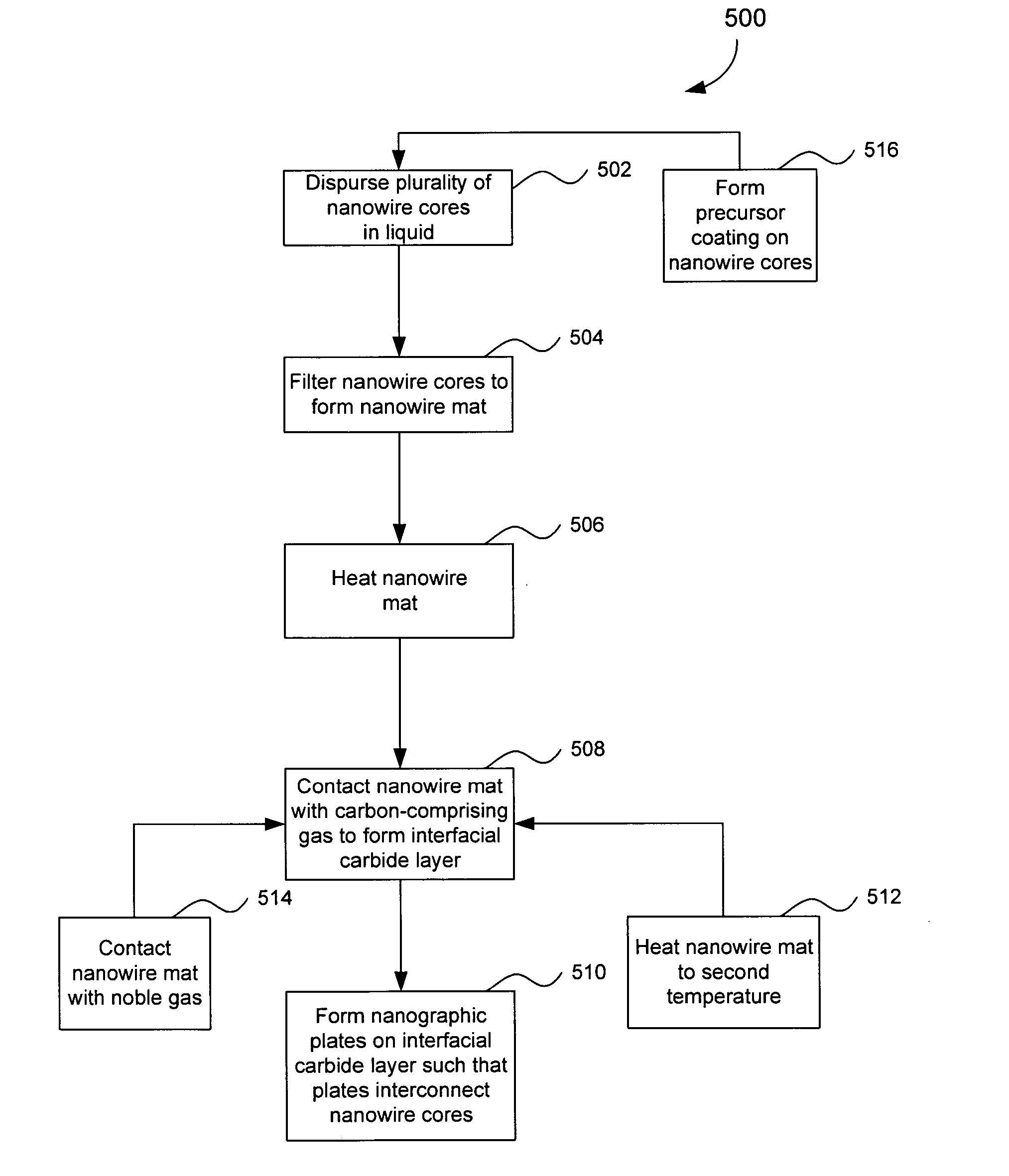
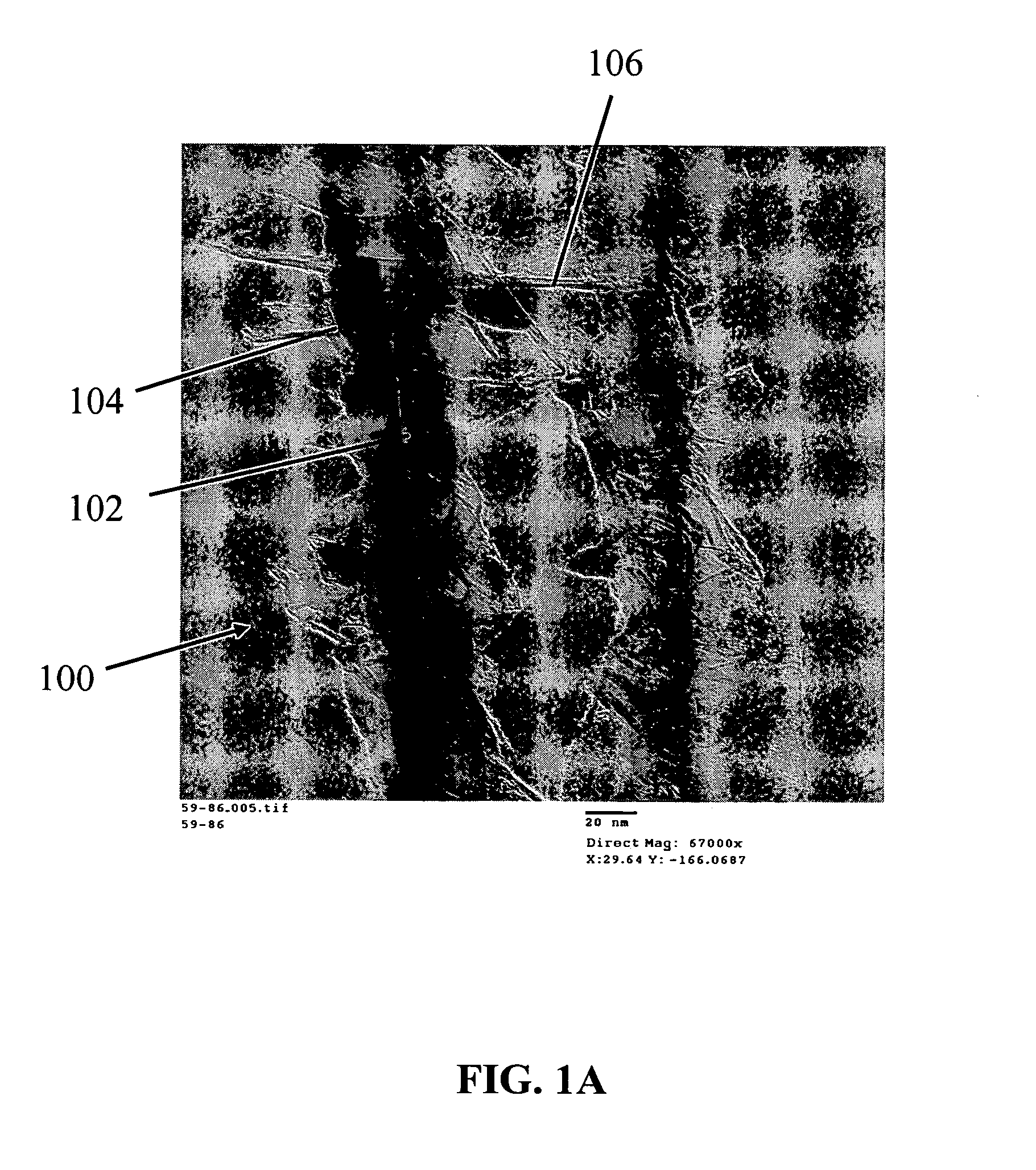
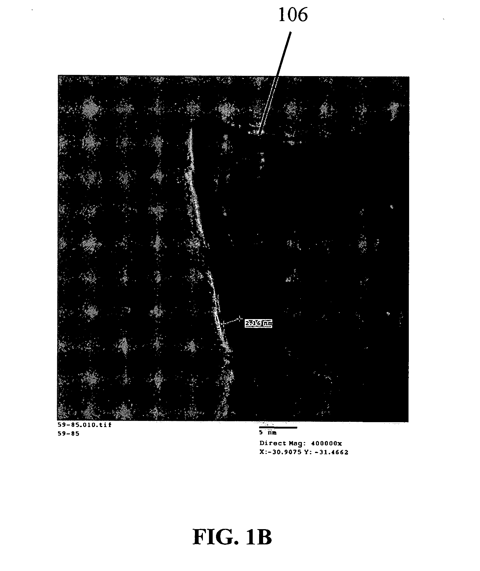
Preparation of Nanowire Structures

[0209] Silicon nanowires coated with WO3 were heated at 650° C. for 30 minutes, followed by 1250° C. for 6 min in the presence of a flowing gas mixture comprising Ar (430 cc / min), H2 (130 cc / min) and CH4 in Ar (228 cc / min). After the preparation was cooled, an interconnected nanowire network 300 comprising interconnected nanowire structures 100 was formed. The nanowire structures 100 comprising Si nanowire cores 102, carbon based layers 104 (SiC / WC interfacial carbide layers) and carbon-based structures 106 (graphene nanographitic plates) connecting the nanowire structures 100.

Example

Example 2

Deposition of Nanoparticles on Nanowires

[0210] Approximately 10 mg Si nanowires were dispersed in ethanol by sonication to form a nanowire suspension. An interconnected nanowire network was prepared by vacuum filtration of the nanowire suspension over a polyvinylidene fluoride (PVDF) membrane and vacuum drying, then 2 cc 0.1% polylysine solution was added to the filter funnel to absorb polylysine on the surface of the nanowires. After 5 minutes, all liquid in the funnel was vacuum removed and the nanowire network was separated from the PVDF membrane. After being dried in an oven at 100° Celsius for 15 minutes, the nanowire network was submerged in 10 cc of Au colloid solution (10 nm colloids) and soaked for 20 minutes to absorb the Au nanoparticles on the surface of the nanowires. Finally, the nanowire network was removed from the Au colloid solution, rinsed with isopropyl alcohol (IPA), and dried at 100° Celsius to obtain a nanowire network coated with gold nanoparticles...

Example

Example 3

Fabrication of Densely Packed Nanowires

[0211] In order to examine methods to increase packing density of nanowires, “bird's-nest” structures of 60 nm silicon nanowires were prepared using various techniques. The results of the methods are represented below in Table 1: TABLE 1Packing Density RelativeMethodto Silicon DensityAs collected on the filter  6%Stirred with shear mixer 6.1%Uniaxially pressed11.2%Surfactant (Triton X-100)  8%Die pressed, 40 KPSI46.6%Compact Packing (90°)78.5%Compact Packing (0°)90.7%

[0212] The packing density prepared by filtering the dispersion of 60 nm nanowires was 6%. Stirring the dispersion with a high speed shear mixer prior to filtration did not improve the packing density. A packing density increase of more than 30% was noted by adding surfactant (Triton X-100) to the nanowire dispersion prior to filtration. A significant increase in packing density was observed after application of uniaxial pressure to the nanowires. A packing density of 4...


PUM


Abstract

The present invention is directed to nanowire structures and interconnected nanowire networks comprising such structures, as well as methods for their production. The nanowire structures comprise a nanowire core, a carbon-based layer, and in additional embodiments, carbon-based structures such as nanographitic plates consisting of graphenes formed on the nanowire cores, interconnecting the nanowire structures in the networks. The networks are porous structures that can be formed into membranes or particles. The nanowire structures and the networks formed using them are useful in catalyst and electrode applications, including fuel cells, as well as field emission devices, support substrates and chromatographic applications.

Description

CROSS REFERENCE TO RELATED APPLICATIONS [0001] The present application is a continuation-in-part of U.S. patent application Ser. No. 11 / 295,133, filed Dec. 6, 2005, which claims the benefit of U.S. Provisional Patent Application Nos. 60 / 634,472, filed Dec. 9, 2004, and 60 / 738,100, filed Nov. 21, 2005. The present application also claims the benefit of U.S. Provisional Patent Application No. 60 / 801,377, filed May 19, 2006, and U.S. Provisional Patent Application No. 60 / 738,100, filed Nov. 21, 2005. The disclosures of each of these applications are incorporated herein by reference in their entireties.BACKGROUND OF THE INVENTION [0002] 1. Field of the Invention [0003] The present invention relates to various nanowire structures, and to interconnected nanowire networks comprising such structures. The present invention also relates to the use of these nanowire structures and interconnected nanowire networks in fuel cells, as field emitting elements and other applications, such as chromat...

Claims


Application Information

Patent Timeline
IPC IPC(8): D02G3/00H01B1/04B05D7/00H01M4/58H01M4/96H01M4/88H01M4/02H01M4/133
CPCH01B1/04H01M4/133H01M4/625H01M4/8605Y02E60/521H01M8/1004H01M8/1097Y10T428/2918H01M4/8657Y02P70/50Y02E60/50Y02E60/10
Inventor NIU, CHUNMING
Owner ONED MATERIAL INC
Why Eureka
Try Eureka