

High-dielectric constant thin film metal oxides on silicon wafers for capacitor applications and methods of manufacture
a technology of thin film metal oxides and silicon wafers, which is applied in the direction of variable capacitors, fixed capacitor details, nuclear engineering, etc., can solve the problems of high surface roughness of foils and ceramic substrates, failure of capacitors with high leakage current densities, and failure of capacitors with lower applied bias voltage, etc., to achieve high packaging density, low cost, and high performance
- Summary
- Abstract
- Description
- Claims
- Application Information
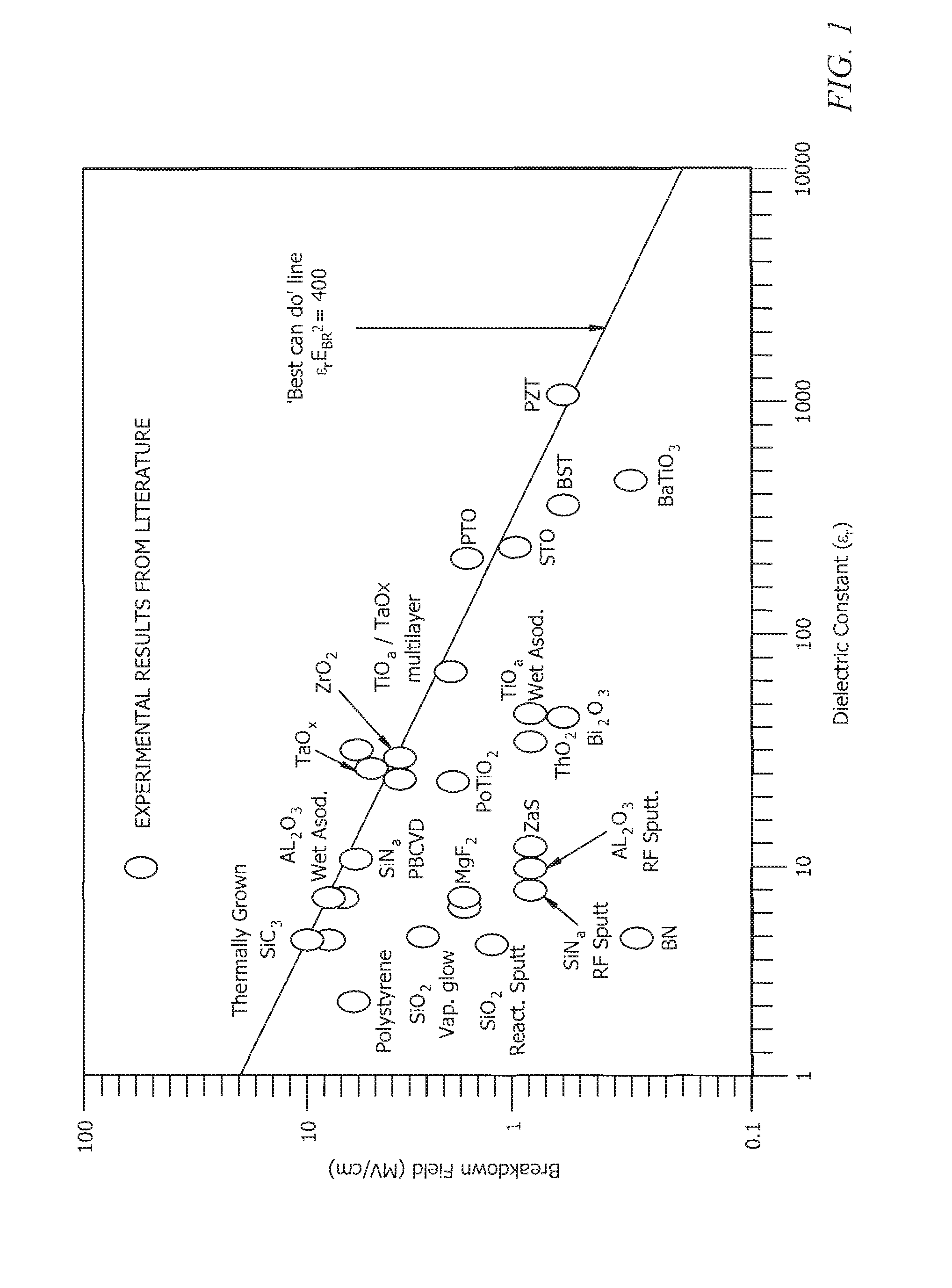
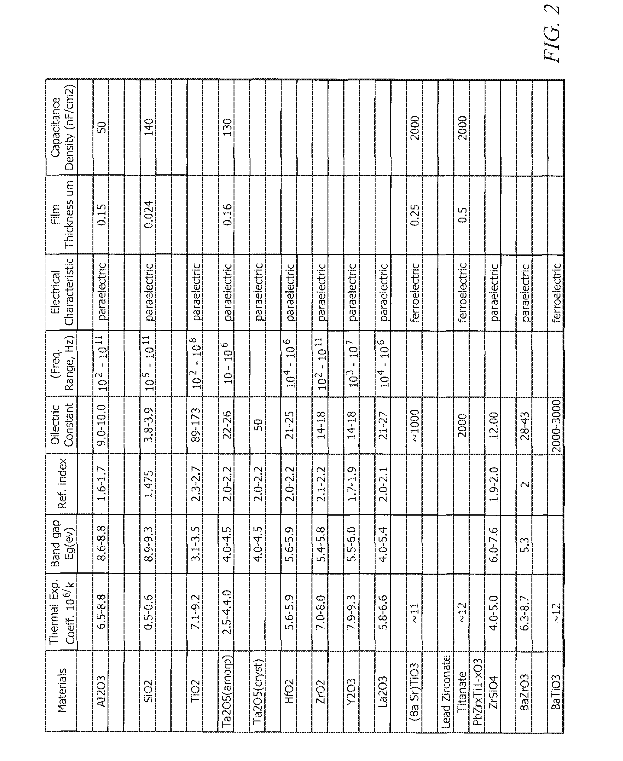
AI Technical Summary
Benefits of technology
Problems solved by technology
Method used
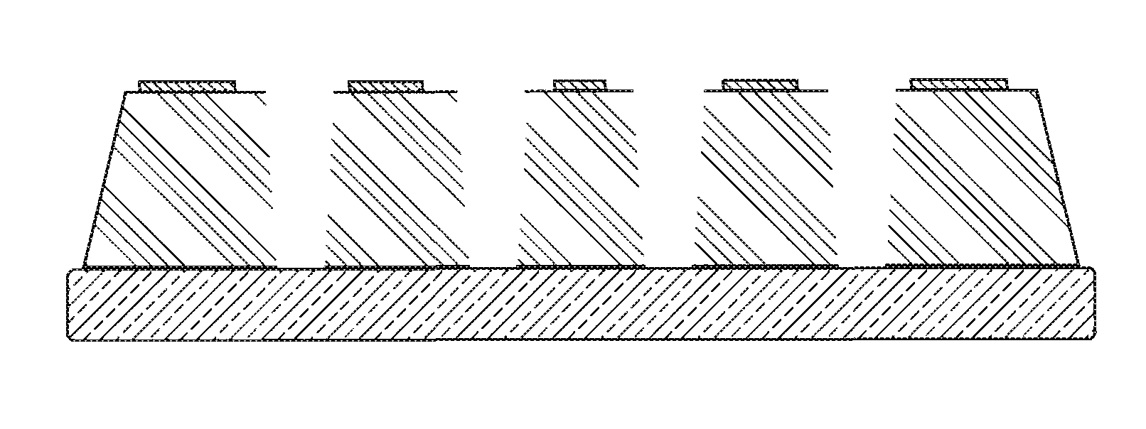
Image

Examples
example i
Step 1
[0115]This step is based on the synthesis of barium titanate itself or a barium titanate precursor such as barium titanate glycolate that is mixed with a block copolymer or other organic templates to make a coating solution that, after deposition, will convert to mesoporous films on subsequent appropriate treatments.
[0116]Preparation of Barium Titanate Glycolate: 5.9 g Barium oxide is placed in a glass beaker, to which 30.0 ml ethylene glycol is added and stirred for an hour. To this, 50 ml of 2 propanol is added and the entire mixture is filtered via vacuum filtration to remove undesired solids. 9.0 g of titanium isopropoxide is added to the recovered liquid, causing the formation of an off-white precipitate. The new mixture is allowed to stir at room temperature for 30 min. The desired solid is then filtered from the mixture via vacuum filtration, washed three times with isopropanol and dried under vacuum.
Step 2
[0117]Preparation of Coating Solution Using Barium Titanate Prec...
example ii
[0120]Preparation of Tantalum Oxide Dielectric Thin Films via Mesoporous Tantalum Oxides:[0121]Synthesis of Mesoporous Tantalum Oxide Solution: 0.18 g acetylacetone, 1.0 g Tantalum ethoxide and 1.33 g 2-propanol were combined and allowed to stir overnight at room temperature. This solution was added to a solution of 0.42 Pluronic P123, 4.66 g 2-propanol and 0.06 g water. Mixture is stirred at room temperature for 1.5 hours, then filtered via 0.2 um PTFE syringe filter.[0122]Deposition of Films: The tantalum oxide precursor solution thus synthesized is spin-coated onto Si and Pt-coated Si wafers with a spin speed of 4000 rpm for 30 seconds. The samples were baked at 130 C for 1 hour followed by a thermal bake at 350 C for 3 hours. Alternatively the TA05 film can be plasma ashed in 02 after the 350c bake, which improves the removal of the organic template.[0123]Infiltration: The post-baked samples (silicon wafers coated with baked tantalum oxide and platinum-coated silicon wafers with...
example iii
Titanium Oxide-Tantalum Oxide films with SiO2 Infiltration (Inverse Opal)
[0127]0.537 g acetylacetone, 1.09 g Tantalum ethoxide, 0.13 g Ti (acac)2 (OiPr)2, and 5.0 g 2-propanol were combined and allowed to stire overnight at room temperature. To this solution was added 0.1 g Pluronic P123, 4.66 g 2-propanol, and 0.06 g water. Mixture is stirred at room temperature for 1.5 hrs, filtered via 0.2 um PFTE syringe filter, and spun onto silicon and platinum-coated silicon wafer substrates (4000 RPM / 30 s).
[0128]These samples were baked at 150 C for 20 min in N2, bubbled through conc. NH3 solution, followed by a 350 C bake for 3 hrs in air.
[0129]Following the bake, samples with silicon and platinum-coated silicon substrates were immersed in a solution of 0.35 g tetraethyl orthosilicate, 0.5 g 0.1 N nitric acid, and 21.5 g ethanol and left to soak overnight.
[0130]After the soak, samples were quickly dip-rinsed with ethanol, and baked at 130 C for an hour. A final firing at 900 C for 2 minutes...
PUM
| Property | Measurement | Unit |
|---|---|---|
| Fraction | aaaaa | aaaaa |
| Mass | aaaaa | aaaaa |
| Mass | aaaaa | aaaaa |
Abstract
Description
Claims
Application Information