The proliferation of electronic devices over the past several years has created problems of radiation containment from these devices.
When not controlled, this radiation can interfere with the normal operating use of other
electrical devices.
However, the problems associated with
electromagnetic interference continue to challenge manufacturers due to the proliferation of devices, increasing
clock speeds, and the increased density of
electronic packaging resulting from continual size reductions in portable devices.
The problems have been further compounded by the increased use of plastic housings.
However, such shells do not necessarily protect the rest of the device from external sources of radiation and design flexibility is limited.
However,
zinc die castings are costly, heavy, and design flexibility is limited.
Sheet
metal liners can be combined with the appeal of a plastic exterior, but sheet
metal liners tend to be expensive and have to be attached to the plastic housing which complicates and lengthens the
assembly process.
Properly molded conductive
fiber loaded plastics offer good shielding performance but suffer from a number of major downfalls.
It also may be difficult to maintain uniformity of
fiber concentration in a final molded part.
Finally, the cost of the fibrous filler is very high, often negating the savings achieved through the
elimination of secondary
processing.
However, these heavily loaded compositions can be difficult to process and other material properties are negatively impacted.
Further, these compositions do not eliminate the other problems associated with using fibers mentioned above.
Unfortunately, injection of plastic resin into a mold cavity typically involves high pressures and shear which can cause destruction to fragile netting or foils.
Clearly, this would be impractical except for the very simplest of geometries.
Unfortunately, the combined operations of
nickel plating, drawing, weaving, annealing and
sintering involved in the grids taught considerably adds to manufacturing cost.
In addition, the insert molding involves preforming of the insert and considerable restriction of the design aspects of the part.
The conductive fibers taught by Daimon and Kanamura are expensive and the
processing to produce the precursor conductive non-woven sheets is complicated.
However, a significant problem arises when one attempts to form more useful three dimensional articles from such sheets, either through
stamping or
thermoforming.
The resin flow and expansion involved in these operations tends to separate and fracture the fibers, resulting in loss of fiber to fiber contact and
conductivity necessary to achieve shielding.
A problem is that the
low melting point metal fibers employed are relatively expensive and manufacture of the precursor sheets is complicated, thereby significantly increasing the cost of the final shaped article.
In addition, significant amounts of trim waste of the expensive sheets can be associated with the
thermoforming operation, further increasing cost.
Further general problems with the use of conductive mats or sheets as shields exist in that they normally end up embedded in the final article, resulting in a non-conductive surface.
This can result in loss of electrical communication along the edges of
mating parts and production of a “
slot antenna”.
Special connectors can be used, but at added cost.
The Hattori U.S. Pat. No. 5,473,111 discussed above proposed to address this problem by extending the shield member outside the periphery of the resin portion of the part, but this is clearly impractical in most cases.
The unique design of the part and die along with the precise
heat control required limits the application of this technique.
In addition, the heat
staking technique does not address the additional “
slot antenna” problem.
In addition, should the
mating surfaces of housing components not contact adequately, a gap is formed in the joint between housing components.
All of these techniques have characteristic disadvantages.
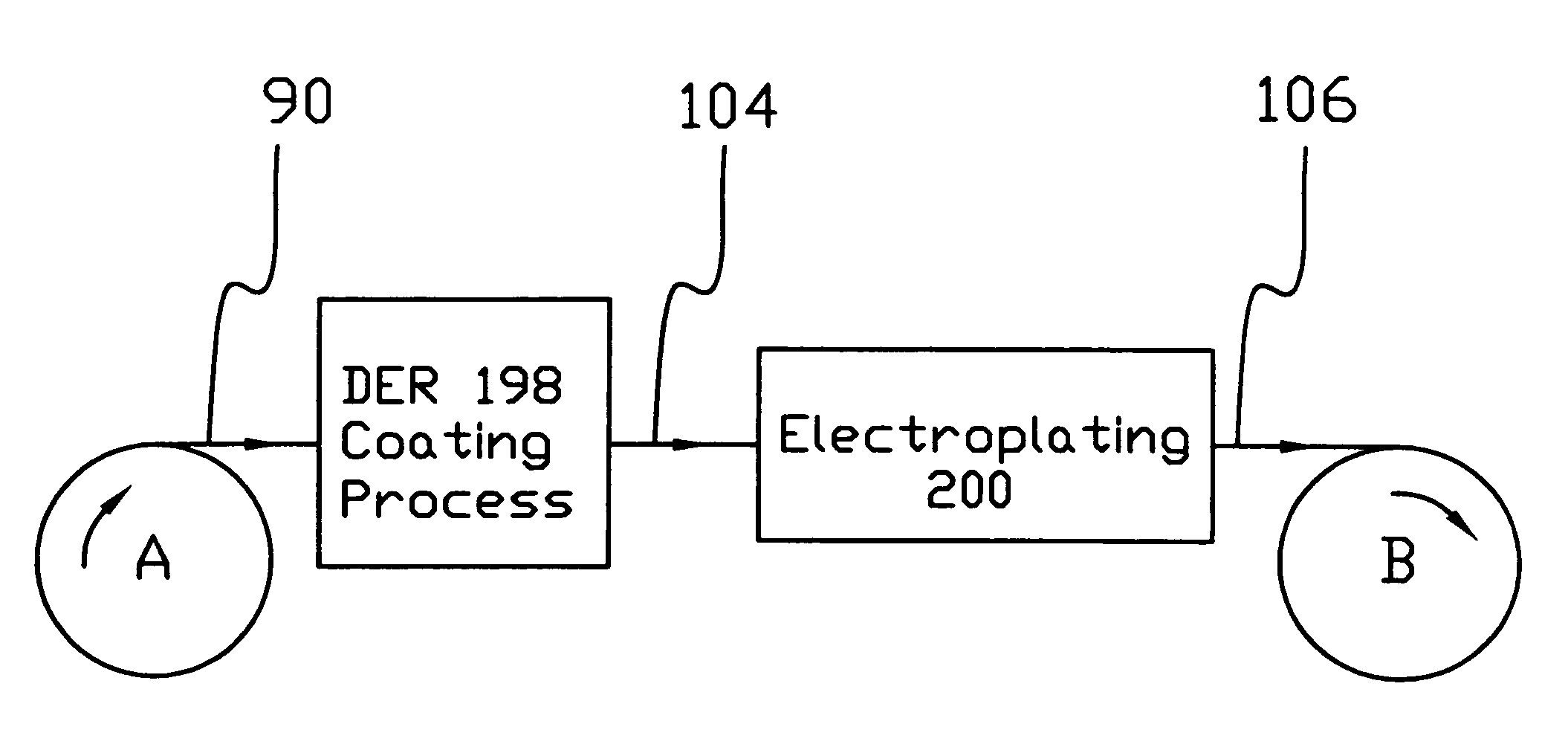
The many steps, expensive materials and the fact that the entire component has to be coated with the specialized electrodeposited
coating severely limit applications of the technique.
As
electronic equipment has evolved, higher frequencies are encountered, and the electrical conductivity imparted by conductive fillers becomes only marginally effective for adequate attenuation of the
high frequency spectrum of the radiation.
These meshes utilize fibers made of relatively expensive materials such as stainless steel,
Monel,
tin-coated
copper, or metal plated polymeric fibers.
In addition, processing of the individual fibers into the mesh adds considerably to the overall cost of the
gasket.
One major
disadvantage of conductive painting is that it is a
line of sight process making it difficult to successfully shield recessed or ribbed areas.
Thin coatings also will not provide good shielding effectiveness so multiple coats may be required.
This may be a particular problem at sharp corners where the well-known “pull-away” characteristic of paints may lead to
slot antenna effects.
Finally, the multiple coats which may be required result in significant material overspray waste, environmental difficulties, and increased costs.
It is also difficult to achieve consistent paint thickness over the surface of an article which can result in variations in shielding performance.
Finally, conductive paints often suffer from problems with durability over time.
Thermoforming is a process limited to parts of relatively simple geometry.
In addition,
vacuum deposition of the relatively thick films required for EMI shielding can be complex and process sensitive, as discussed in the Gabower U.S. Pat. No. 5,811,050.
The many steps employing harsh and expensive chemicals make the process intrinsically costly and environmentally difficult.
The process comprises many steps and is very sensitive to processing variables used to fabricate the plastic substrate, limiting applications to carefully molded parts and designs.
It may be difficult to properly mold conventional plateable plastics using the rapid injection rates often required for the thin walls of electronic components.
The rapid injection rates can cause poor surface distribution of etchable species, resulting in poor
surface roughening and subsequent inferior bonding of the chemically deposited metal.
Finally, selective metallizing can be difficult, especially on complex parts, since the
electroless plating may tend to coat any exposed surface unless the overall process is carefully controlled.
Efforts to advance systems contemplating metal electrodeposition directly onto the surface of an
electrically conductive polymer have encountered a number of obstacles.
The first is the combination of fabrication difficulty and material property deterioration brought about by the heavy filler loadings often required.
A second is the high cost of many conductive fillers employed such as silver flake.
In some cases such as
electroforming, where the electrodeposited metal is eventually removed from the substrate, metal /
polymer adhesion may actually be detrimental.
However, in most cases sufficient adhesion is required to prevent metal / polymer separation during extended environmental and use cycles.
However, here the metal particles are generally encapsulated by the resin binder, often resulting in a resin rich “
skin”.
An additional major obstacle confronting development of
electrically conductive polymeric resin compositions capable of being directly electroplated is the initial “bridge” of electrodeposit on the surface of the electrically conductive resin.
However, if the
contact resistance is excessive or the substrate is insufficiently conductive, the electrodeposit current favors the rack tip to the point where the electrodeposit will not bridge to the substrate.
Moreover, a further problem is encountered even if specialized
racking successfully achieves electrodeposit bridging to the substrate.
The polymeric substrate can be relatively limited in the amount of electrodeposition current which it alone can convey.
In a fashion similar to the bridging problem discussed above, the electrodeposition current favors the electrodeposited metal and the lateral growth can be extremely slow and erratic.
This restricts the size and “growth length” of the substrate conductive pattern, increases plating costs, and can also result in large non-uniformities in electrodeposit integrity and thickness over the pattern.
However, attempts to make an acceptable directly electroplateable resin using the relatively small metal containing fillers alone encounter a number of barriers.
First, the fine metal containing fillers are relatively expensive.
The loadings required to achieve the particle-to-particle proximity to achieve acceptable conductivity increases the cost of the polymer / filler blend dramatically.
The metal containing fillers are accompanied by further problems.
They tend to cause deterioration of the mechanical properties and processing characteristics of many resins.
This significantly limits options in resin and fabriation selection.
A required heavy loading of metal filler severely restricts ability to manipulate processing properties in this way.
A further problem is that metal fillers can be
abrasive to processing machinery and may require specialized screws, barrels, and the like.
Finally, despite being electrically conductive, a simple metal-filled polymer still offers no mechanism to produce adhesion of an electrodeposit since the metal particles are generally encapsulated by the resin binder, often resulting in a non-conductive resin-rich “
skin”.
For the above reasons, fine
metal particle containing plastics have not been widely used as substrates for directly electroplateable articles.
A fundamental problem remaining unresolved by the Adelman teaching is the relatively
high resistivity of carbon loaded polymers.
Thus, the electrodeposit bridging and coverage rate problems described above remained unresolved by the Adelman teachings.
Conventional “electroless” plating technology does not permit broad compositional flexibility.
Conventional “electroless” plating technology does not permit great flexibility to “custom formulate”.
Due to multiple performance problems associated with their intended end use, none of the attempts identified above to produce a directly electroplateable plastic has ever achieved any recognizable commercial success.

