Plasm-aided selenium sulfuration treatment device and process

A plasma and vulcanization treatment technology, applied in metal material coating process, semiconductor devices, gaseous chemical plating, etc., can solve the problems of thin film crystalline quality or structure, poor reactivity, low band gap, etc. High conversion efficiency, increased reactivity, and the effect of reducing heating temperature

Inactive Publication Date: 2011-05-11
NANKAI UNIV
View PDF4 Cites 17 Cited by
  • Summary
  • Abstract
  • Description
  • Claims
  • Application Information

AI Technical Summary

Problems solved by technology

But it has the following disadvantages: 1). The gaseous selenium formed by the solid-state selenium (or sulfur) source is mostly composed of Se 5 、Se 6 、Se 7 exist in the form of macromolecular groups or atomic clusters, and H 2 Compared with Se, the reaction activity is poor, the process is complicated, the reaction temperature is high, and it is close to the softening point of the glass substrate; 2). When the solid source selenium (or sulfide) is gasified, the gas is generated from a certain position. For large-area As far as the substrate is concerned, it is not easy to form a uniform distribution, and the uniformity of the formed film is very poor, which is difficult to be used for large-scale industrialization; 3). When the prefabricated layer metal Cu, In, and Ga are converted into compound semiconductor film materials, almost every The interrelationships between the atoms have changed, from the interatomic metal bond to the covalent bond. On the other hand, the selenium atom reacts with the metal prefabricated layer, its volume changes, and the interface in contact with Mo is displaced. , resulting in a severe decline in the binding force between the CIGS thin film and the Mo back electrode, which affects the next process of the semiconductor thin film battery and the quality of the final thin film device; 4). Metal gallium is generally formed in the form of copper gallium alloy and indium by sputtering to form a prefabricated layer , metal indium in the film is more likely to react than gallium during selenization, so it is easy to form CuInSe 2 , instead of Cu(In,Ga)Se 2 , causing Ga atoms to be driven to the bottom layer. On the other hand, Ga is more likely to combine with Mo, and Ga diffuses to the back electrode of Mo and cannot form a compound semiconductor. The open circuit voltage and photoelectric conversion efficiency are not high
[0006] The common disadvantages of gas phase selenium sulfide and solid source selenium sulfide are that the crystal quality or structure of the film is loose, the compactness is poor, the semiconductor polycrystalline film has many defect states, and the photoelectric conversion efficiency of the thin film battery is low.

Method used


Image

  • Plasm-aided selenium sulfuration treatment device and process
  • Plasm-aided selenium sulfuration treatment device and process
  • Plasm-aided selenium sulfuration treatment device and process

Examples


Embodiment 1

[0033] Selenium vulcanization treatment of embodiment 1 Cu-In metal prefabricated layer

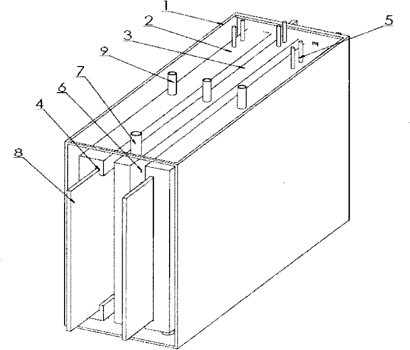
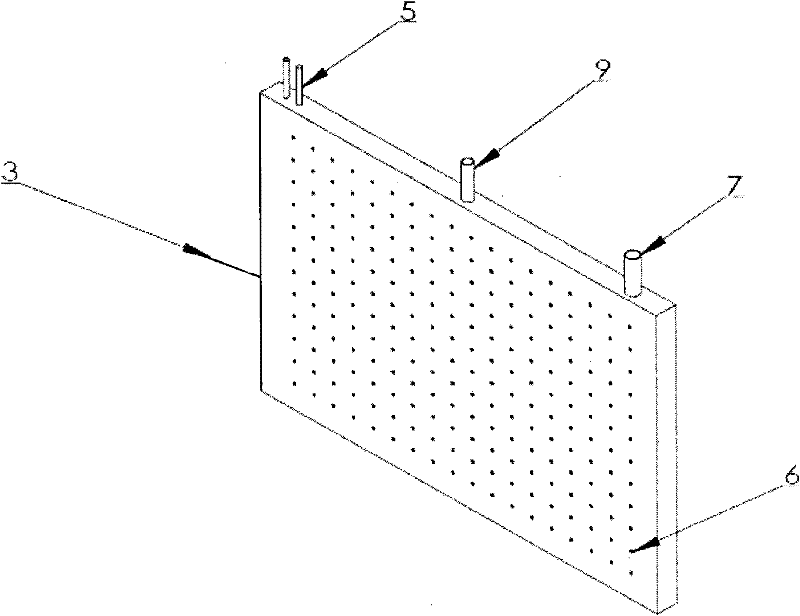
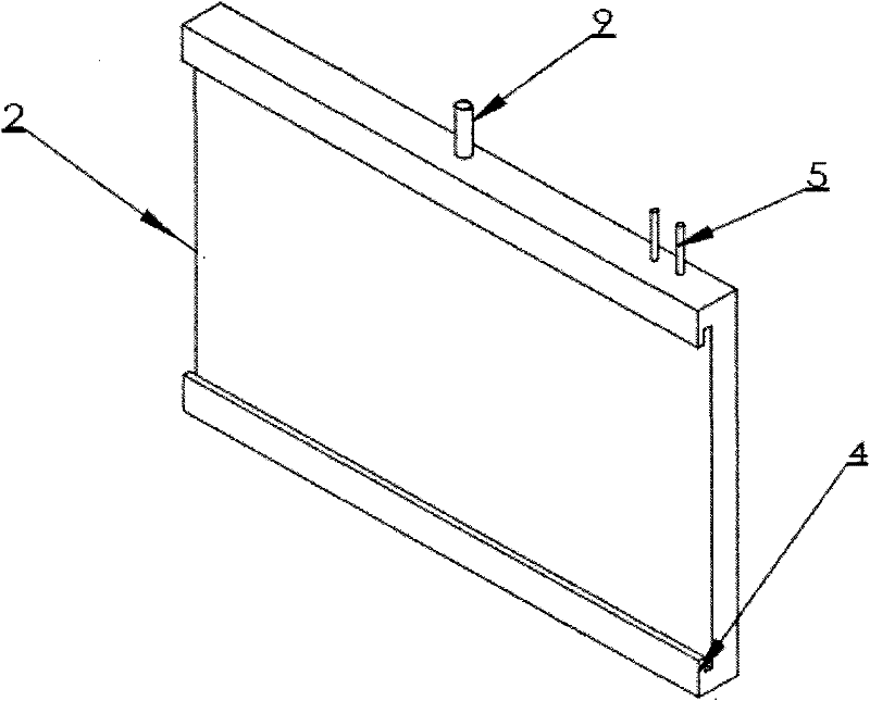
[0034] Sputter and deposit 0.6-1.4 μm thick metal Mo on ordinary soda-lime glass, use laser scribing, and then sputter or evaporate a layer of NaF (thickness 0.1-0.3 μm) (or Na 2 S), then sputtering deposit copper indium or copper indium alloy, the atomic ratio (Cu / In) of copper and indium is 0.85: 1.0~0.95: 1.0, put them into the base on the cathode in the capacitively coupled parallel plate radio frequency plasma device On the sheet rack 4, close the vacuum chamber to evacuate. When the mechanical pump is linked with the molecular pump or the vacuum diffusion pump, the vacuum reaches 10 -2 ~10 -5 Pa, start the heating device inside the cathode plate and the anode plate, wherein the temperature change of the cathode plate is as follows Figure 4 shown. That is, let the battery substrate 8 evenly heat up at a rate of 0.5-2°C / s, and after stabilizing at about 100°C for 10-20 minutes, c...

Embodiment 2

[0037] Example 2 CuIn 0.3 Ga 0.7 Selenization Treatment of Metal Prefabricated Layer

[0038] The pre-preparation process of the electrode on the surface of the battery substrate is the same as that of Example 1. A layer of NaF (thickness 0.1-0.3 μm) (or NaF) (or NaF) is sputtered or evaporated on the surface of the Mo film. 2 S), and then sputtering deposited copper-gallium alloy (CuGa 0.3 , thickness 0.8~1.2μm), sputtering deposited indium (0.5~0.8μm), or copper-gallium-indium layered deposition respectively, the total chemical ratio should satisfy Cu(Ga 0.3 In 0.7 ) Se 2 , and requires Cu / (In+Ga)=1:1.0~1:1.15, this is because indium gallium has a certain transformation loss in the selenization process, and the doping of sodium ions is beneficial to reduce the copper indium gallium metal prefabricated layer selenium The crystallization temperature, grain growth and flatness of the film surface during the chemical transformation process increase the carrier concentration...

Embodiment 3

[0042] Embodiment 3CIGS carries out selenium vulcanization

[0043]The CIGS semiconductor thin film formed after selenization of CuInGa metal pre-set layer, if vulcanized, can form wide bandgap, high resistance, n-type homogeneous pn junction, which can improve the quality of CIS and CIGS thin film. In this embodiment, according to the method of embodiment 2, in the later stage of preparing CIGS thin film material by plasma-assisted selenization, the composition of the gas is changed to input Ar+H 2 S or Ar+S+H 2 Finally, sulfur-containing high-resistance Cu(In 0.7 Ga 0.3 ) (SeS) layer, use EDX (energy dispersive X-ray analyzer) to test the depth of the surface layer of the sulfur-containing film, and determine the sulfur-passing time (3-10min) to control its thickness at 10-20nm; this sulfur-containing surface film It constitutes an n-type semiconductor layer or a high-resistance layer of CIGS that is wider than the forbidden band width of the underlying CIGS film, and the...


PUM

PropertyMeasurementUnit
pore sizeaaaaaaaaaa
thicknessaaaaaaaaaa
thicknessaaaaaaaaaa

Abstract

The invention relates to a plasm-aided selenium sulfuration treatment device arranged in a vacuum chamber. The plasm-aided selenium sulfuration treatment device comprises a shell, a cathode plate and an anode plate, wherein the cathode plate and the anode plate are alternately stacked to form a plasm generator, the cathode plate is provided with a groove for fixing a semiconductor film substrate, and small holes are uniformly distributed on the surface of the anode plate which is provided with a gas pipe, an independent internal heating electrode and an anode temperature-measuring point. The process based on the treatment device comprises the following steps of: (1) precasting a metal layer on the semiconductor film material according to the proportions of a chemical formula and then putting in the groove of the cathode plate; and (2) putting in the vacuum chamber to vacuumize, switching on a power supply to heat the cathode plate and the anode plate, switching on a power supply of the plasm generator and adding the mixed gases of selenium or sulfur, hydrogen and argon. The invention has the advantages that selenium ions have high reaction activity, the selenizing reaction of the metal precast layer is complete, the photoelectric conversion efficiency is high, and the substrate has lower heating temperature and is hardly deformed. An electronic mode is adopted to monitor the change of capacitive reactance between the two electrodes, know the conversion development and reduce the defective index of the industrial production.

Description

technical field [0001] The invention relates to a solar cell film material preparation technology, in particular to a plasma-assisted selenium vulcanization treatment device and process. Background technique [0002] copper indium selenide (CuInSe 2 Abbreviated as: CIS) or copper indium gallium selenide [Cu(InGa)(SeS) in which gallium and sulfur are solid-dissolved 2 Abbreviated as: CIGS] solar thin-film battery is a photovoltaic device composed of deposited multi-layer thin films on the substrate of ordinary soda-lime glass or polyimide film, metal sheet (aluminum, stainless steel, molybdenum foil, etc.). The structure is generally: glass substrate / metal molybdenum (Mo) back electrode / light absorbing layer (CIGS) / buffer layer [CdS, ZnS, ZnSe, In(OH) 3 , ZnS(O, OH), etc.] / high resistance intrinsic i-ZnO / conductive window layer [doped ZnO(ZnO:Al, ZnO:Ga, ZnO:B), SnO 2 , ITO (indium tin oxide), etc.] / metal grid electrode / anti-reflection film, etc. Wherein the quality that ...

Claims


Application Information

Patent Timeline
Patent Type & Authority Applications(China)
IPC IPC(8): C23C16/50C23C16/52C23C16/30H01L31/18
CPCY02P70/50
Inventor 孙国忠敖建平李宝璋张超何青周志强
Owner NANKAI UNIV
Why Eureka
Try Eureka