A self-powered nanosensor based on piezoelectric-friction coupling effect
A nano sensor and coupling effect technology, applied in the field of nano technology and sensing, can solve the problems of unstable output performance of nano generators, achieve good friction power generation performance, broad application prospects, and simplify the structure
- Summary
- Abstract
- Description
- Claims
- Application Information
AI Technical Summary
Problems solved by technology
Method used
Image
Examples
preparation example Construction
[0031] The preparation of the nanowire structure adopts one or more of nanoimprinting technology, electron beam direct writing technology, focused ion beam direct writing technology, laser direct writing technology, spinning process and wet etching process.
[0032] The material of the structural layer is polydimethylsiloxane, poly(vinylidene fluoride-trifluoroethylene), carbon nanotubes, fluorinated ethylene propylene, polytetrafluoroethylene, polyimide, polyethylene terephthalate One of ester, polyvinylidene fluoride, polyvinylidene fluoride, polymethyl methacrylate and mercapto-ene.
[0033] The material of the electrode layer is one of gold, silver, aluminum, copper, nickel, indium tin oxide and conductive fiber.
[0034] The preparation of the electrode layer adopts one or more of sputtering, spin coating, bonding and evaporation processes.
[0035] Support and protection layers are made of nylon, fabric, dimethicone, polyimide, silicon, polymethyl methacrylate, polyethy...
Embodiment 1
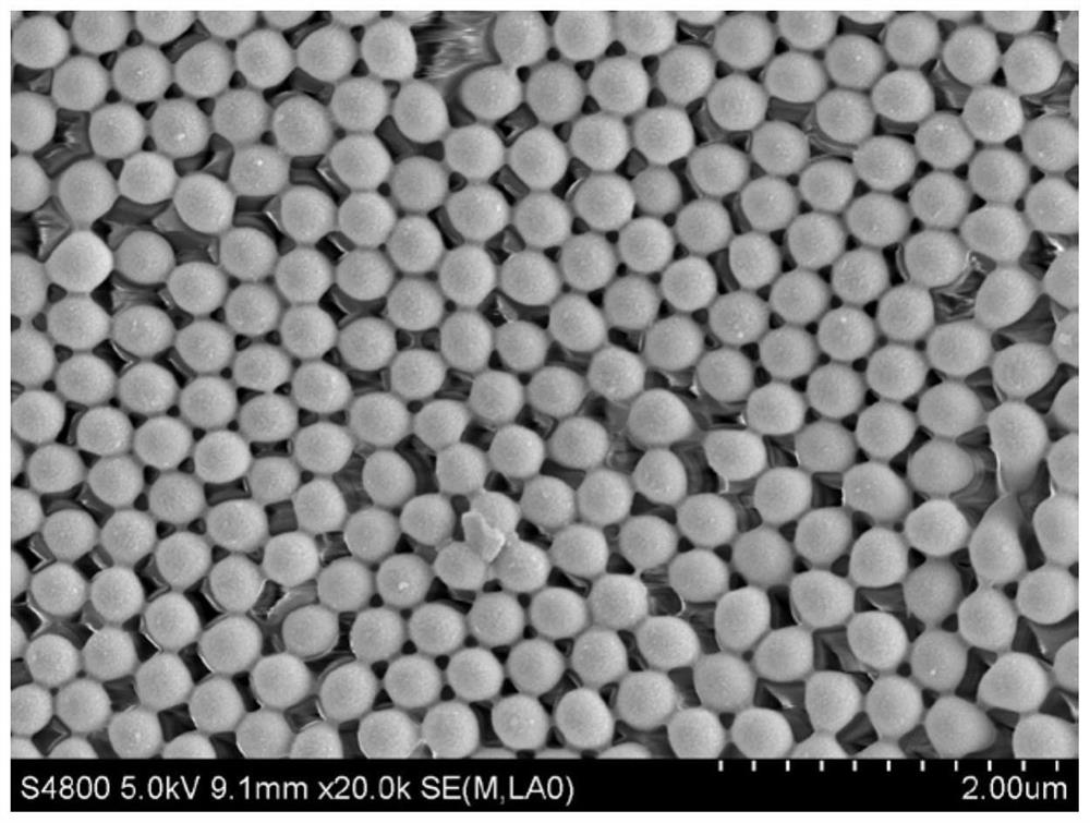
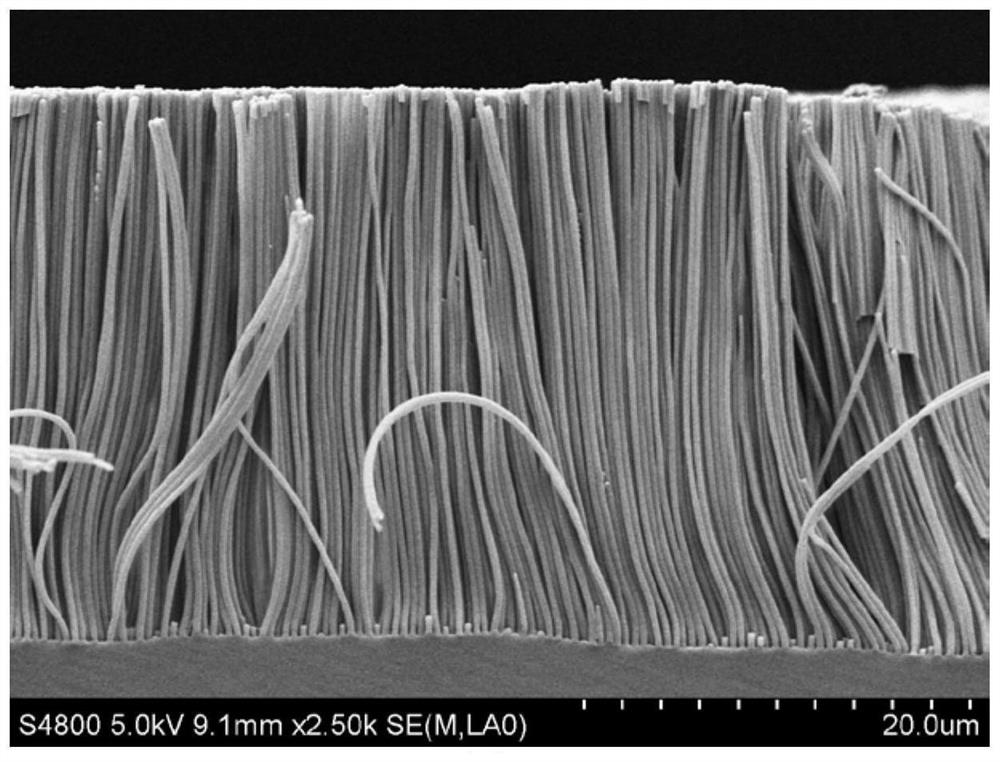
[0041] The material of the piezoelectric-friction coupling layer of the self-powered sensor is polydimethylsiloxane material, and the surface is covered with a nanowire array structure. The diameter of the nanowire is 280 nanometers, the length is 30 micrometers, and the aspect ratio is greater than 100:1. Scanning electron micrographs of the upper surface and cross-sectional structure of the nanowire structure are shown in figure 2 and 3shown. The nanowire structure adopts hot pressing nanoimprinting technology combined with wet etching process. The thermal curing temperature is 90 degrees Celsius and the curing time is 2 hours. The wet etching process uses 80% sodium hydroxide solution and the etching time is 5 hours. The thickness of the entire piezoelectric-friction coupling layer is 1 mm, the material of the electrode layer is indium tin oxide, and the thickness is 200 nm, and the material of the supporting layer between the two electrode layers is polyethylene terephth...
Embodiment 2
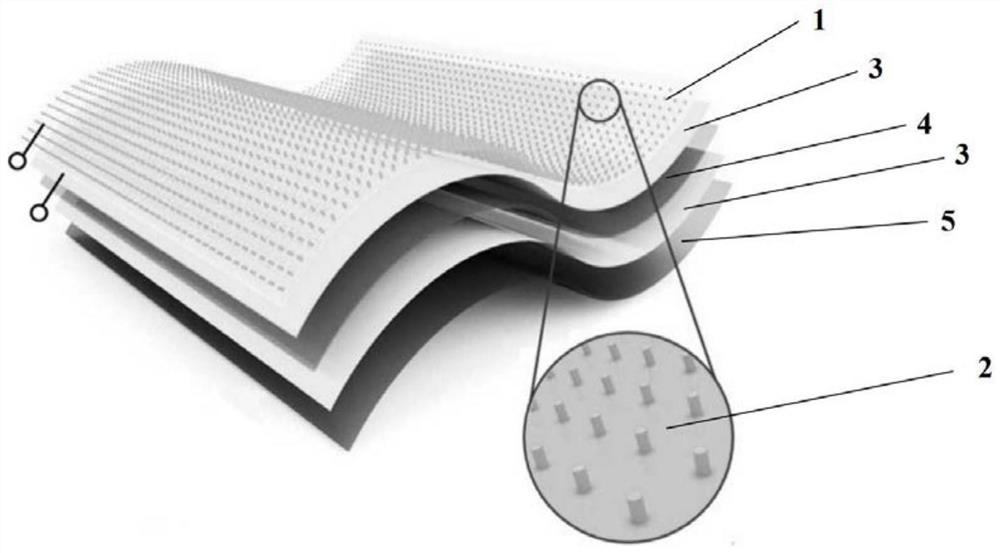
[0044] like figure 1 The self-powered sensor based on the pressure-friction coupling effect is shown. The material of the piezoelectric-friction coupling layer is a mercapto-ene material, and the surface is covered with a nanowire array structure. The diameter of the nanowire is 100 nanometers and the length is 3 microns. The aspect ratio is 30:1, and the cross-sectional scanning electron micrograph of the nanowire structure is shown in Figure 4 shown. The nanowire structure adopts nanoimprint technology combined with wet etching process. The imprint based on flexible template does not need to provide external pressure. The wavelength of ultraviolet light is 365 nanometers, and the exposure intensity is 20mW / cm 2 , the curing time is 1 minute, the wet etching process uses a sodium hydroxide solution with a concentration of 80%, and the etching time is 10 hours. The thickness of the entire piezoelectric-friction coupling layer is 1 mm, the material of the electrode layer is ...
PUM
| Property | Measurement | Unit |
|---|---|---|
| size | aaaaa | aaaaa |
| thickness | aaaaa | aaaaa |
| thickness | aaaaa | aaaaa |
Abstract
Description
Claims
Application Information


