[0035] In the context of this disclosure, field-transistors typically have a
gate oxide greater than 0.5 microns, but may be as thin as 0.1 microns. Field transistors may be constructed using either a polysilicon or
metal gate layer deposited over a thick, grown,
thermal oxide. Many existing
CMOS technologies include a
LOCOS-based oxidation step in which a thick
oxide is grown from a
silicon wafer surface in defined areas; field transistors may be formed on this thick
oxide formed during
LOCOS. An excellent overview of well-known
integrated circuit and
CMOS processing techniques and well-known fabrication processes may be found in the three volume series: Wolf, S., R. N. Tauber,
Silicon Processing for the VLSI Era: Volume 1 Process Technology, Lattice Press,
Sunset Beach Calif., 1986; Wolf, S.,
Silicon Processing for the VLSI Era: Volume 2
Process Integration, Lattice Press,
Sunset Beach Calif., 1990; Wolf, S.,
Silicon Processing for the VLSI Era: Volume 3 The Submicron
MOSFET, Lattice Press,
Sunset Beach Calif., 1995. Note that a field transistor may be formed on top of either the native substrate material or a tub or well of similar or opposite
doping type to the native substrate material. Alternative configurations, not using a
LOCOS-based
gate oxide for example, include a
metal gate transistor in which the
metal gate is formed over an active region, but includes a thick, depositied
oxide layer (deposited as a pre-metal
dielectric after poly deposition) above the active region; a
metal gate transistor in which the
metal gate is formed over a deposited oxide which lies upon a LOCOS oxide; a poly or
metal gate transistor in which the gate is formed on top of an additional thermally-grown oxide thicker than the thickest
low voltage gate oxides available on
chip through an additional oxidation step. It should be understood that there are many ways of forming a field transistor and that the precise method of forming and constitutive materials of the field transistor should not be limited to the exemplary structures described above. While an
advantage of the present invention is that in most cases a field transistor may be formed using existing implanted
layers and thermally grown oxides, it should also be clear that separate
implant or masking
layers (for example to effect a field threshold adjust, or source / drain extension
layers) or separate
gate oxide growth steps may be added to an existing process flow to form field transistors.
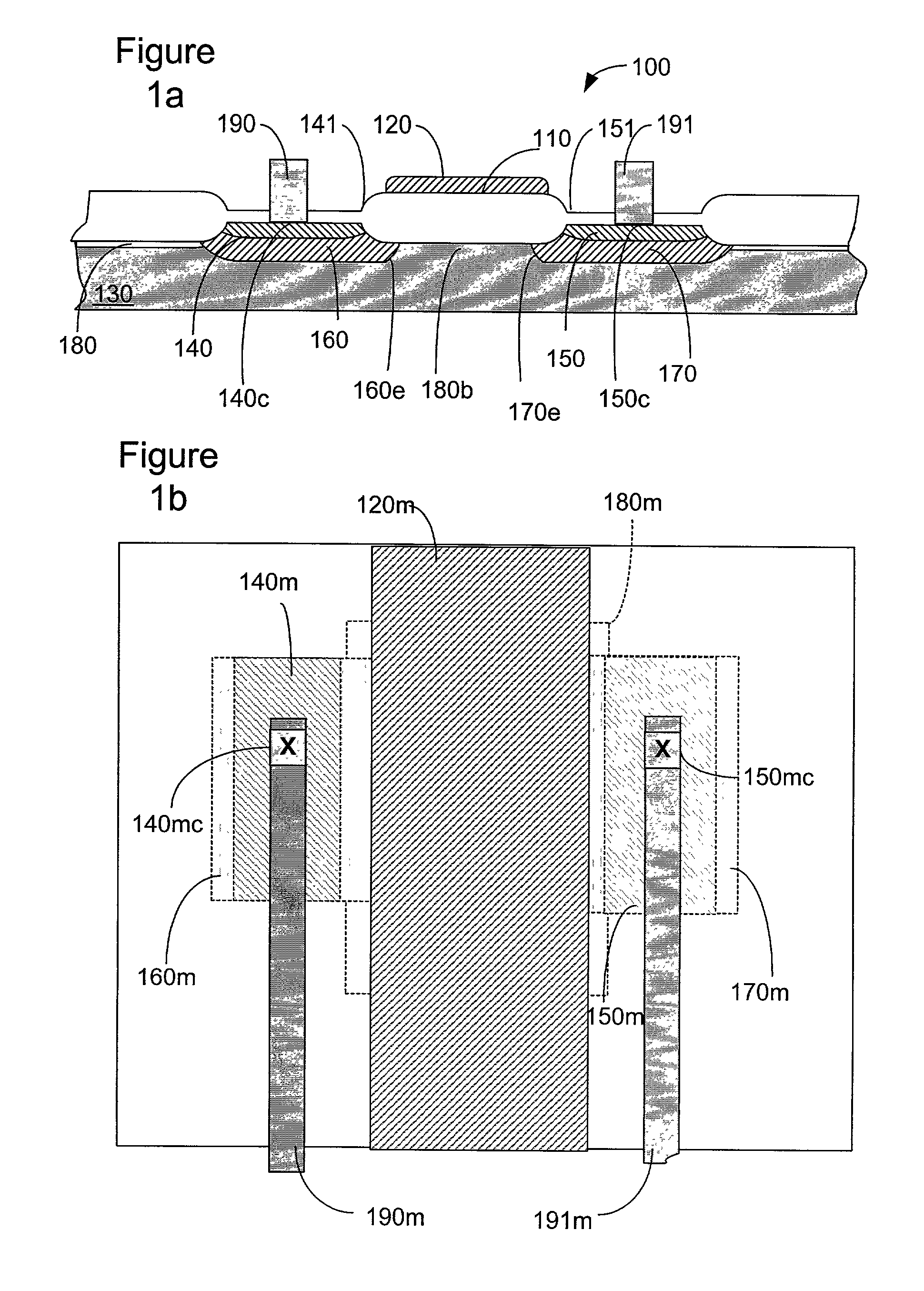
[0036] FIG. 1a shows one embodiment of a PMOS field transistor in accordance with the present invention. FIG. 1b shows a simplified diagram of
mask layers of one particular
layout of a field transistor 100. In this embodiment, the transistor structure is formed over a
field oxide region 110 such as one which may be formed using a LOCOS (LOCal Oxidation of Silicon) or
SILO (Sealed-Interface Local Oxidation) process, for example. In this particular embodiment of a field transistor, the gate 120 (defined by
mask data 120m) comprises a polysilicon conductor deposited on a LOCOS oxide 110.
Oxide 110 is physically defined by regions where a protective
nitride layer (formed on a pad-oxide layer to reduce stress-effects in subsequently-formed low-voltage transistors) is absent during LOCOS oxidation. The gate oxide is a thermally-grown oxide (formed, for example, during a LOCOS step at 1100 C. in steam for approximately 4.5 hours) having a thickness of 1.5 .mu.m. Substrate 130 is 10
Ohm-cm <100> n-type
silicon, the source 140 and drain 150 implants are p+
boron implants (Defined by
mask data 140m and 150m --a combination of active and p+ select). Source / drain extension areas 160, 170 are formed from diffused P-wells (defined by mask data 160m 170m --pwell).
Metal conductors 190, 191 make contact to the source and drain regions by contacts 140c and 150c (metal conductors defined by mask data 190m 191m and contacts defined by mask data 140mc and 150mc). A field threshold adjust block region 180b (defined by mask data 180m) is also shown. In this embodiment of a
field device, the field threshold adjust block region 180b blocks channel-stop implants (in this case
arsenic, or an n-type
dopant) intentionally introduced to raise the field
threshold voltage of parasitic transistors. The channel-stop
implant is typically used to prevent parasitic field transistors from being turned on in low-voltage portions of circuits, regions 180 for example. In an alternative embodiment, the field block region is not present and the PMOS field threshold is equal to the field threshold of transistors in the low-voltage portions of circuits. In yet another embodiment, implantation of a p-type
dopant may be added to region 180b to lower the magnitude of the field threshold of the PMOS field transistor, or make the transistor into a depletion-mode device.
[0037] It should be noted that to maintain a high
breakdown voltage in this field transistor, the active area edges 141 and 151 are spaced several microns from the edge of the gate 120. Because well-
implant typically occurs before LOCOS formation, source / drain extension areas 160e and 170e are easily constructed using a standard p-well
diffusion. Extension regions 160e, 170e help ensure that control gate 120 can form a
conductive channel that stretches from the source to the drain, uninterrupted. A complementary field transistor may be constructed by reversing the polarity of the
dopant types and changing the polarity of the local substrate through well / tub implants. When a source / drain extension implant is unavailable in a particular process, an additional implant step may be added in the process of forming the transistor in order to fabricate a device with the correct device polarity. Alternatively, the area between the
active edge and the gate may be minimized and the fringing fields from the gate may be used to turn on the field transistor; however the performance of a device constructed in this fashion may be inferior. In yet another embodiment, existing implants such as Nfield (PMOS channel-stop) or Pfield (NMOS channel-stop) may be used as source-drain extension areas: i.e. for an NMOS device, formed in a pwell, source drain extension areas may be formed from PMOS channel-stop (n-type dopant). As described above, a field transistor may also be constructed using a metal gate with a deposited interlayer or pre-metal
dielectric (ILD or PMD) between the metal gate and an active region wherein the active region comprises a thin, thermally-grown gate oxide. Standard n+ or p+ (as appropriate) implants used for low-voltage transistor source / drain implant may, in this case, be used to form a source-drain extension region for the field transistor.
[0038] Field devices formed in accordance with the foregoing description and having a structure as outlined in FIGS. 1a and 1b are used in embodiments of a high voltage amplification apparatus as discussed herein. In the context of the invention, embodiments may be described with respect to a particular construction as NMOS or PMOS. It should be recognized that the particular technology used to fabricate a particular device is described by way of example and complementary devices may be used in each instance of an NMOS or PMOS device.
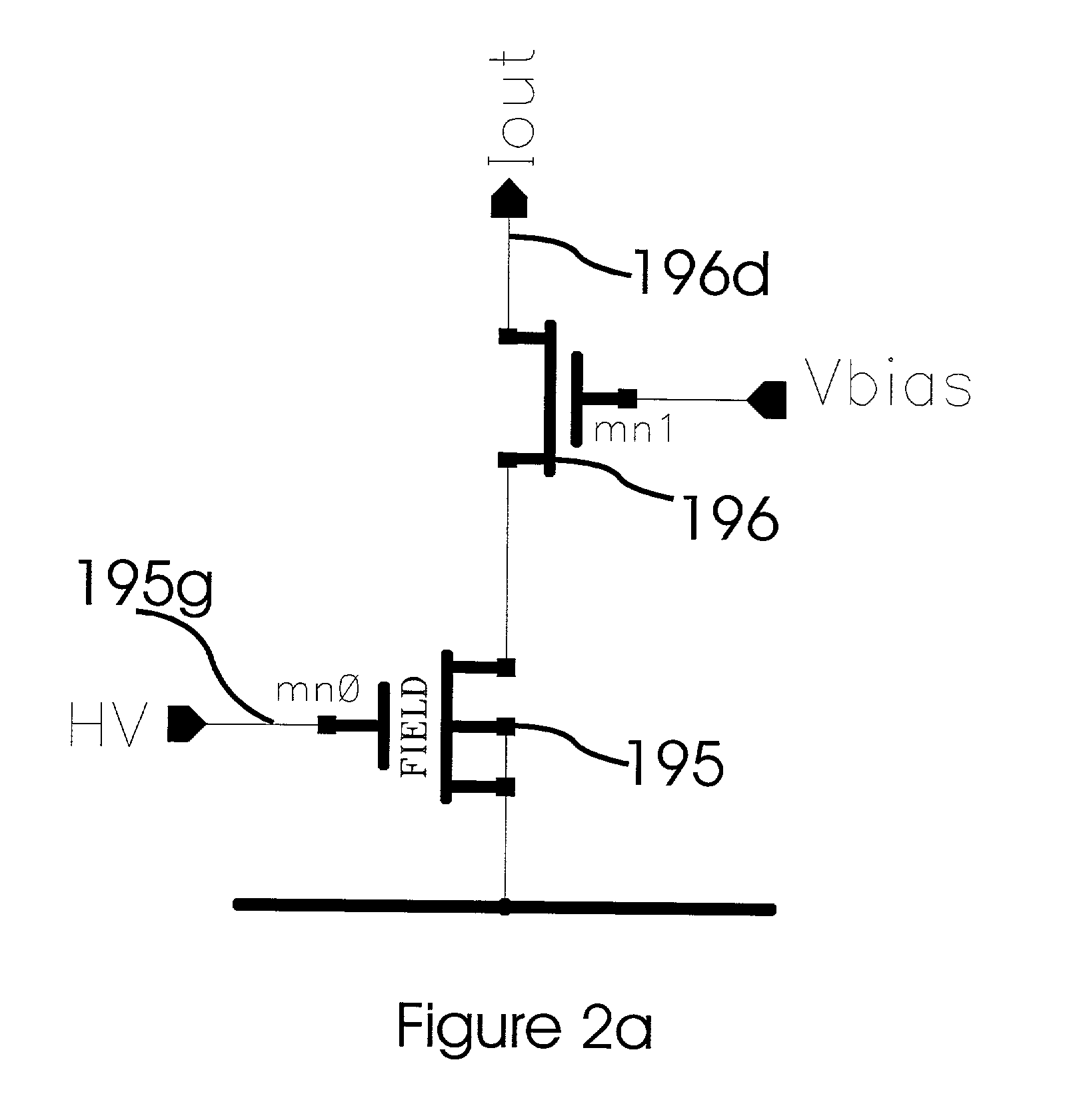
[0039] FIG. 2 shows a first embodiment of the invention. A single NMOS field transistor 195, formed in a complementary manner to the PMOS field transistor shown in FIG. 1a, has a high-voltage terminal 195g and is cascoded by low voltage NMOS transistor 196. A bias voltage V.sub.Bias is applied to the gate of transistor 196, causing a substantially
constant voltage to appear across the drain and source of transistor 195. Assuming that the conductance of transistor 196 is substantially larger than the conductance of transistor 195, field transistor 195 is in
triode. Thus, for voltages V.sub.HV applied to terminal 195g an output current appears at terminal 196d approximated by: 1 I out C ox( w l ) ( V HV - V T195 )( V Bias - V T196 )
[0040] where V.sub.T196 is the
threshold voltage of transistor 196, V.sub.TI95 is the
threshold voltage of transistor 195, and w, I, .mu., and C.sub.ox are the width, length, mobility and
capacitance per unit area of transistor 195, respectively. Note that the output current of transistor 195 is proportional to the input voltage V.sub.HV, and thus may be used to sense a high voltage in a small area using devices found in a standard
CMOS process and drawing small amounts of power. The output current may be connected to a transimpedance stage, (such as a
resistor or, alternatively, an opamp placed in
negative feedback with a
resistor between the negative input terminal and the output terminal), to obtain an output voltage representative of the high-voltage input.


