

Composite oxide sintered body and sputtering target comprising same
a composite oxide and sputtering technology, applied in the direction of diaphragms, metallic material coating processes, conductive materials, etc., can solve the problems of difficult to form a crystalline silicon thin film on a glass substrate or an organic substrate, a large amount of energy and a large number of steps are required to produce a crystalline silicon thin film, etc., to achieve the reproducibility of the resulting thin film transistor, reduce the bulk resistance of the composite oxide sintered body
- Summary
- Abstract
- Description
- Claims
- Application Information
AI Technical Summary
Benefits of technology
Problems solved by technology
Method used
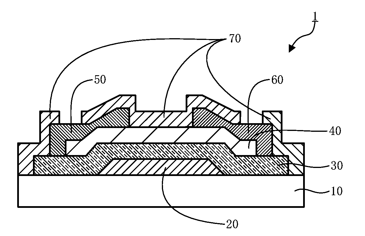
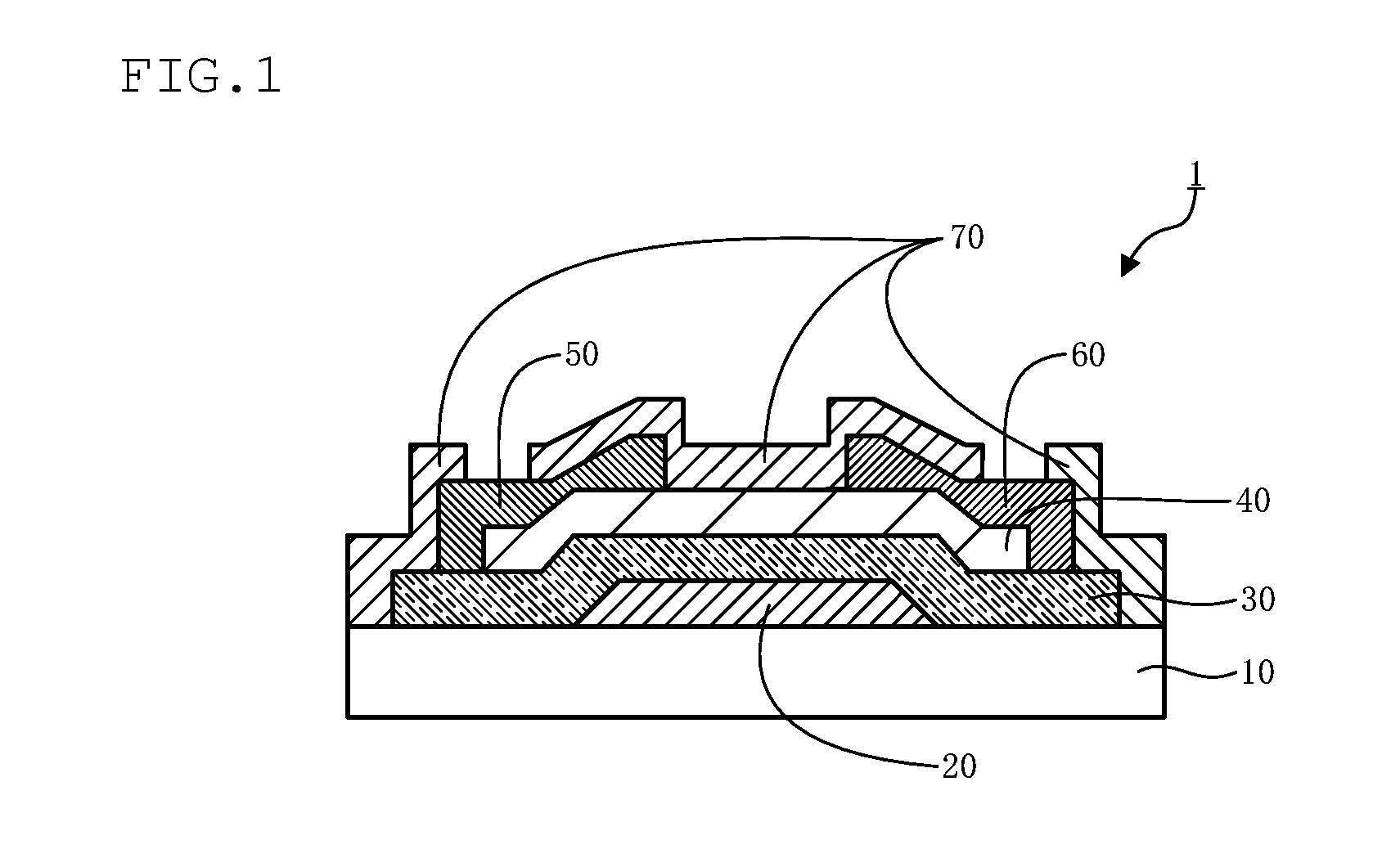
Image

Examples
example 1
[0180]Production of Composite Oxide Sintered Body
[0181]The following oxide powders were used as starting raw material powders. The specific surface area of each powder was measured by the BET method.
[0182](a) Indium oxide powder (4N, specific surface area: 8 m2 / g)
[0183](b) Tin oxide powder (4N, specific surface area: 8 m2 / g)
[0184](c) Zinc oxide powder (4N, specific surface area: 5 m2 / g)
[0185]The oxide powders were weighed and mixed so that the atomic ratio “(a):(b):(c)” was 35:15:50 to prepare a raw material powder mixture. The raw material powder mixture had a specific surface area of 6.3 m2 / g.
[0186]The raw material powder mixture was mixed and ground using an agitator bead mill with a wet medium while checking the specific surface area of the powder mixture. The specific surface area of the ground powder mixture was larger than that of the raw material powder mixture by 2 m2 / g.
[0187]Zirconia beads having a diameter of 1 mm were used as the media of the agitator bead mill with a we...
examples 8 to 13
[0213]A sintered body and a target were produced in the same manner as in Example 1, except that the oxide powders were weighed in an atomic ratio shown in Table 3, and sintered under the following conditions. The results are shown in Table 3.
Temperature increase rate: 1° C. / min
Sintering temperature: 1480° C.
Sintering time: 12 hours
Processing: Each side of a sintered body having a thickness of 9 mm was ground by 2 mm.
[0214]The sintered body obtained in each example was subjected to X-ray diffraction analysis. The results are given below.
example 8
The Sintered Body Mainly Included a Bixbyite Structure Compound Shown by In2O3 and a Spinel Structure Compound Shown by Zn2SnO4
PUM
| Property | Measurement | Unit |
|---|---|---|
| diameter | aaaaa | aaaaa |
| average crystal grain size | aaaaa | aaaaa |
| specific surface area | aaaaa | aaaaa |
Abstract
Description
Claims
Application Information