Thus a similar charging mechanism
underlay both the earlier UV flood process and the Pt “flash gate”; unfortunately, neither of these processes provided adequate stability, nor did subsequent improvements and refinements successfully resolve the surface
passivation problem.
A key part of the difficulty lay with the
oxide.
Unfortunately, the “flash
oxide” failed to stabilize the device, as changing environmental conditions (especially with respect to
exposure to
hydrogen) could reverse the polarity of the chemisorbed charge with a catastrophic effect on
detector quantum efficiency and
spectral response.
In particular,
chemisorption charging is unstable with respect to the ionizing effects of deep
ultraviolet light, which is well known to liberate H+ ions and create traps in SiO2 and other
dielectric layers used as insulating layers in the
semiconductor industry.
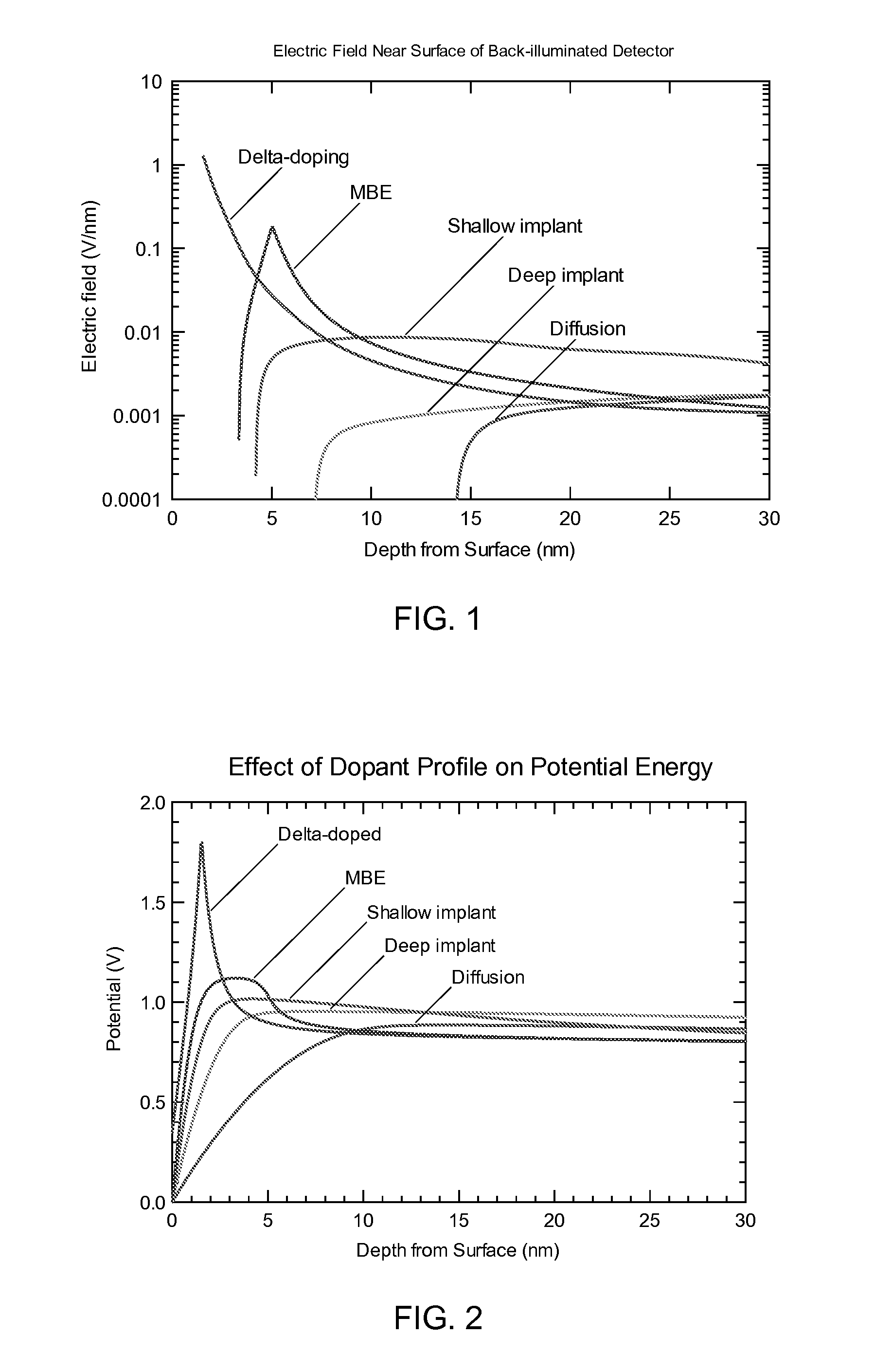
As shown in FIG. 2, surface
doping methods necessarily produce a back surface
potential well, in which minority carriers may be trapped and lost due to recombination.
Most of the implanted atoms are not located on electrically active lattice sites of the
crystal, and the implantation process creates a
high density of defects that degrade the quality of the semiconductor.
However, the annealing temperature required for
dopant activation is incompatible with the thermal constraints of device
processing (note that there are isolated exceptions, in which
refractory metals are used in the front-surface
electronics in order to enable high-temperature furnace anneals of
ion-implanted layers; however,
refractory metals require specialized processes and impose constraints on
metal conductivity that are not compatible with all imaging device technologies and applications).
Third, detectors are sensitive to variations in surface doping, so that
ion implantation and
laser annealing processes applied to back-illuminated imaging detectors require optimization to achieve uniform
quantum efficiency over the entire
detector surface.
This is particularly challenging for
laser annealing, which tends to create “
brick wall” artifacts in imaging detectors.
However, this is only a relative
advantage, as the
physics of
ion implantation and the necessity of maintaining process compatibility with imaging detectors provide only limited flexibility in designing the shape, depth, peak position, amplitude, and uniformity of the dopant profile.
These constraints in turn place limits on the ability to use
ion implantation for optimization of detector performance, especially with regard to UV
quantum efficiency, defect-related
dark current generation, and “deep depletion” for improved spatial resolution.
In particular,
ion implantation cannot create abrupt dopant profiles, which are extremely important for surface passivation.
FIG. 1 and FIG. 2 illustrate this inability to provide abrupt dopant profiles, as the electric fields and surface potential barriers formed by
ion implantation are significantly weaker than other forms of surface doping, such as MBE growth.
The inability of ion implantation / anneal processes to create abrupt dopant profiles is a limitation that extends beyond the field of imaging detector technologies.
Achieving abrupt dopant profiles is one of the major challenges faced by the
semiconductor industry in its ongoing efforts to fabricate integrated circuits with higher densities.
One of the limitations lies with broadening of implanted dopant distributions during the annealing process.
The observed high rates of
diffusion are related to defects inevitably created by the implantation process.
However, despite significant advances in the two decades following the development of WF / PC 2 detectors, the state-of-the-art ion-implanted devices in WFC3 still exhibit
quantum efficiency hysteresis (QEH) that is outside the HST specifications.
This solution is limited to imaging applications in which the detector is cooled to cryogenic temperatures, which is impractical for many commercial applications, nor does this solution provide adequate stability for detectors illuminated by UV lasers.
This precision is the ultimate in abrupt doping profiles and cannot be achieved by ion implantation or any other conventional doping process (e.g., ion implantation and
diffusion).
Even with the incorporation of
hydrogen passivation, the observed
dark current is still an
order of magnitude higher than an equivalent front-illuminated device, indicating that back-surface defects are not fully passivated.
The slowly varying dopant profiles created by
diffusion and ion implantation produce weak, slowly varying electric fields and potentials, which provides poor isolation of surface from bulk and leads to instabilities in the response (as seen in the WFC3 detector performance data from the Hubble Space
Telescope).
This reliance on low defect densities presents a problem for stability, because
ionizing radiation is well known to degrade devices by forming surface defects, which are electrically active defects (also known as traps) that exist in both the
oxide and at the silicon-oxide interface.
Stability is an important performance metric, as charging and discharging of surfaces and interfaces can play havoc with devices.
This presents a problem for at least two reasons: first, because
conductivity is an essential function of the substrate that should be reproduced by the surface passivation layer; and second, the low
surface conductivity indicates that the
delta-doped surface is less robust than previously thought.
Delta-layers buried deep under the surface are not suitable for surface passivation of imaging detectors, because too much
signal is lost in the surface region.
An effort has been made to make use of accepted models and to incorporate as much detail and knowledge of materials as is practical; nevertheless, devices and methods described here are to be evaluated based on characterization and performance data, and do not stand or fall based on accuracy of the models.
In addition, 3D doping at ultrahigh concentrations results in local distortions of the silicon
crystal lattice due to strain, which causes the formation of electrical states in the bandgap that act as traps and recombination centers.
In other words, bulk (3D) doping reaches a limit, wherein attempting to increase the dopant concentration beyond the limit is not effective for surface passivation.
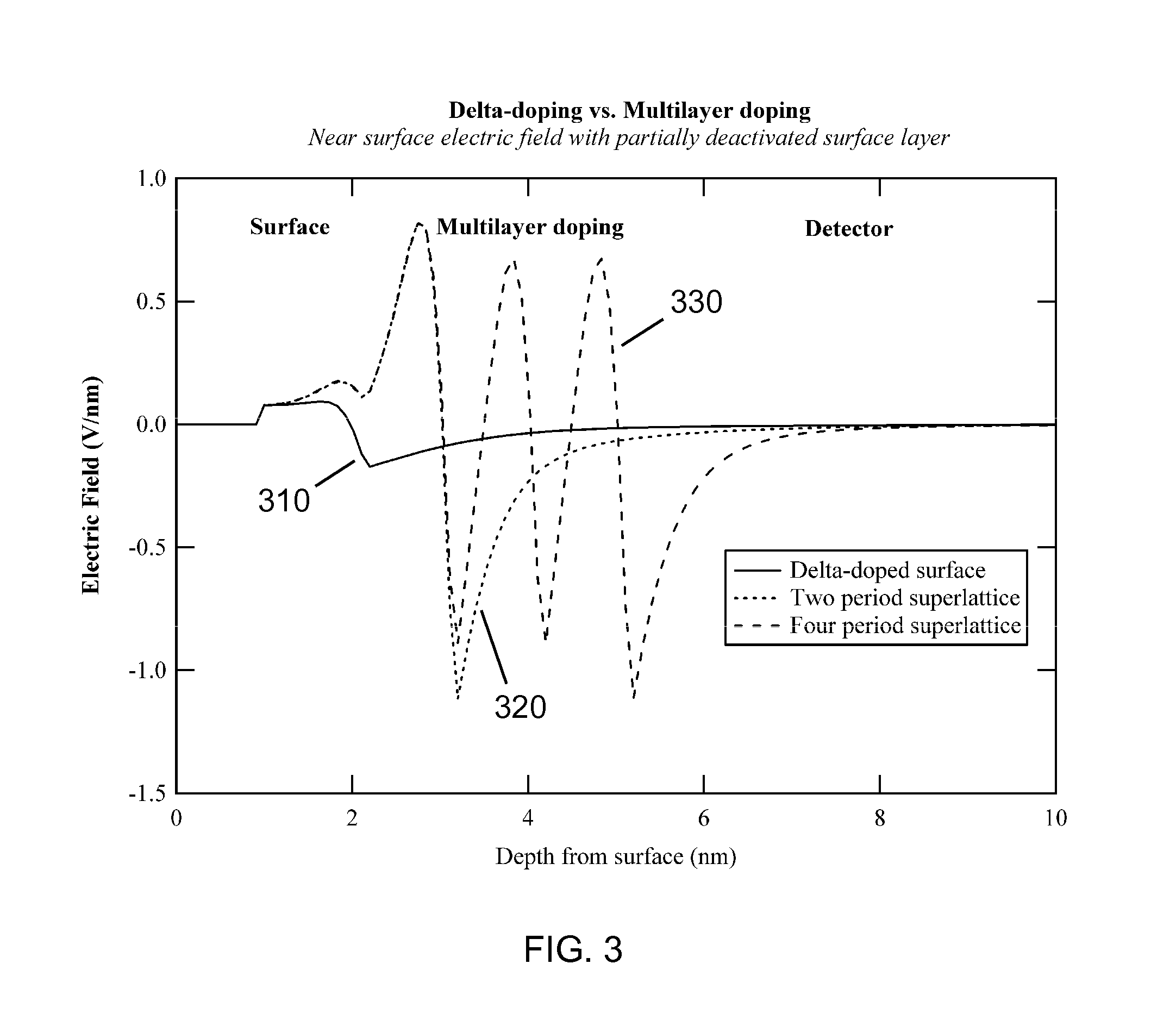
If the separation between layers is too large carriers could get trapped in the individual wells, and the quantum efficiency would be low.
The
dipole layer creates an
electric field that tends to confine holes in the semiconductor and electrons at the surface; however, the
dipole layer is so narrow that quantum confinement greatly increases the
ground state energy of electrons confined at the surface, to the point that most of the states are coupled to
conduction band states in the bulk of the detector.
Note however that whereas
delta-doping provides the highest potential barrier of all other methods in the prior art,
delta-doping is potentially subject to increased tunnel-assisted
dark current generation due to the thin barrier separating the Si—SiO2 interface from the bulk silicon.
These states have the ability to trap photogenerated electrons at the surface, where they are subject either to loss due to recombination, or to re-emission giving rise to imaging artifacts.
However, deactivation of dopants in the layer nearest the surface has caused the formation of a wider
surface layer, and there are a small number of states that could trap electrons and thereby lead to a reduction in quantum efficiency.
However, in both
delta doping (FIG. 10) and multilayer doping (FIG. 12), high densities of interface traps cause the formation of a deep surface well, resulting in the existence of
surface states that could trap electrons and thereby lead to a reduction in quantum efficiency.
Although 3D doping appears to provide a narrower backside well at low interface trap densities, this is probably not physically accurate because of a well-known effect of deactivation of near-surface dopants by the infusion of
hydrogen into the silicon.
Moreover, the width of the backside
potential well for 2D doping is everywhere less than a nanometer, which means that electrons do not behave classically in this regime.
Quantization of the
valence band results in confinement of holes in states localized to the vicinity of the multilayers, while quantization of the
electron states in the backside well results in
surface states that are most often not fully confined to the region of the interface.
ce. As described in FIG. 26, there is no compelling reason to move the doped layers deeper into the silicon—in fact, it may result in a loss of efficiency—but it is nevertheless interesting to examine the
physics of
electron trapping at the interface in terms of the design parameters of multilayer dop
o shown. Second, careful study of FIG. 26 and FIG. 27 reveals that an additional hole state has also
Such
exposure is well known to damage silicon detectors by increasing the density of interface traps.
In the ion implanted surface, the depth of surface
potential well increases dramatically with increasing interface
trap density, resulting in low, unstable quantum efficiency for heavily damaged surfaces.
However, heavily damaged MBE 3D surfaces form a backside potential well that is wide and deep enough to exhibit degradation and instabilities in detector quantum efficiency.
However, delta-doping is subject to the design tradeoffs discussed above, and, as we shall see, delta doped surfaces are vulnerable to other damage mechanisms (e.g., UV-induced oxidation).
Methods for measuring dopant profiles, such as
secondary ion mass spectrometry (SIMS), cannot resolve the dopant profiles within multilayer doped surfaces.
The location of this limit indicates that it is not possible to eliminate surface
trapping of electrons using 3D doping methods without exceeding the limit beyond which
material quality and device performance deteriorate.
Comparison of FIG. 37 with FIG. 36 shows that quantum exclusion cannot be achieved by 3D doping profiles with dopant densities that are below the 3D doping limit, beyond which
material quality deteriorates.
It is well known in the art that photons are more damaging at higher energies.
As a result of the energy-dependence of degradation mechanisms, increasing the
photon energy results in damage occurring at lower integrated fluxes.
The damage observed on EIT is typical of silicon detectors exposed to FUV, EUV, and x-
ray radiation, in which accumulated damage to the Si—SiO2 interface leads to charging and instabilities of the detector surface.
Trap formation is cumulative, and potentially irreversible, which is one reason why surface and interface passivation technologies that rely on initially low defect densities, such as thermally grown oxides and
hydrogen passivation, may not remain stable under UV illumination.
No method of surface doping can prevent this type of degradation, including multilayer 2D doping.
However, multilayer 2D doping uniquely makes the detector performance immune from
radiation-induced changes in the interface
trap density.
In space, solar cells are exposed to deep and
far ultraviolet light, which is far more damaging.
Consequently, for low illumination intensities, UV-induced trap formation is not expected to be a significant
threat to the stability of the multilayer 2D doped surface.
This is in sharp contrast with
chemisorption charging, which is vulnerable to permanent band-flattening due to accumulation of interface and oxide trapped charge, enhanced surface-generated dark current due to trap formation at the Si—SiO2 interface, and hot-carrier induced degradation of chemisorbed charge.
High quality, low defect oxides do not ensure long-term stability, as UV-induced damage is known to cause the formation of traps.
Second,
immunity from interface
trap density creates a great deal of freedom in designing and depositing AR coatings.
As of the present time, no other fabrication technique has been successful in developing stable AR-coated devices in this spectral range.
Second, a single delta-doped layer is vulnerable to increased surface dark current due to tunneling if the delta layer is too close to the surface.
The failures of ion-implanted and chemisorption-charged devices to survive DUV
laser illumination can be understood in terms of DUV-induced changes to the interface trap density, although in the case of chemisorption-charging there may be additional damage mechanisms.
At 263 nm, absorption in the oxide is negligible, and damage occurs primarily through hot carrier degradation of the interface.
No other existing device was able to achieve anything close to this stability.
Other detectors processed using state-of-the-art surface passivation technologies failed at significantly lower integrated fluxes.
At 193 nm, a fraction of the photons are absorbed in the oxide, potentially producing damage by directly breaking bonds in the oxide, in addition to damage caused indirectly by
exposure of the interface to hot carriers generated by absorption in the
silicon detector.

