Method and apparatus for dicing of thin and ultra thin semiconductor wafer using ultrafast pulse laser

a technology of ultra-thin semiconductor wafers and ultra-thin semiconductor wafers, applied in metal working apparatus, manufacturing tools, welding/soldering/cutting articles, etc., can solve the problems of thin ic packaging dicing, die chipping and breakage, and severe backside chipping, so as to improve the quality improve the accuracy of dicing, and improve the effect of top surface and inner wall quality

Inactive Publication Date: 2005-12-15
LASERFACTURING
View PDF27 Cites 226 Cited by
  • Summary
  • Abstract
  • Description
  • Claims
  • Application Information

AI Technical Summary

Benefits of technology

[0034] In another aspect of the present invention, the pulse energy plays a vital role in micro and nano processing with high quality. The pulse energy required to ablate a feature depends on the depth of ablation, repeatability of feature size required and the feature quality. The maximum depth that can be generated for a given focused spot size of the laser beam depends on the pulse energy. As the ablated feature becomes deeper it is difficult to remove the ablated material from the hole and hence the ablated material absorbs the energy of the subsequent pulse. Also the uncertainty in the feature size obtained will depend on the number of pulse required to ablate the required feature. Due to the topography generated and debris deposited in the crater by the ablation of the first pulse the absorption of the successive pulse is different due to the defects generated in the previous pulse, scattering of the laser beam etc. Due to the above mechanism the ablation threshold of the successive pulse may be vary. The uncertainty in the diameter of the ablated feature increases with increase in the number of pulses. Also, higher pulse energy generates sufficient pressure for ejecting the debris out of the carter and hence the successive pulse will interact with the fresh substrate. This results in improved top surface and inner wall quality of the ablated feature. Hence it is advantageous to higher pulse energy and lower number of pulse to ablate a required feature.
[0035] In another aspect of the invention, the effect of wavelength on the cutting efficiency and stability of micron and nano processing using laser pulse from ultrafast laser oscillator is disclosed. In ultrafast laser processing the wavelength

Problems solved by technology

But as the thickness of the wafer decreases below 100 micrometer, saw dicing leads to chipping and breaking of the dies.
Alternatively the silicon is diced by saw and ground to the desired thickness, but this process leads to severe backside chipping during the grinding process.
Concerns about ultra-thin IC packaging dicing include wafer breakage.
Even a small force will cause breakage, the worst case in semiconductor manufacturing.
Below the thickness of 50 μm contact dicing method is not feasible due to wafer breakage.
Water is extreme harmful, and round corners are required to enhance the die strength
But as the thickness of the wafer decreases below 100 micrometer, saw dicing leads to chipping and breaking of the dies.
Alternatively the silicon is diced by saw and grinded to the desired thickness, but this process leads to severe backside chipping during grinding process.
A long pulse laser increases the dicing speed and reduces the dicing kerf width, but it has limitations due to long pulse width (nanosecond pulse width).
The problems of this technique include chipping and micro cracks.
Moreover, the heat affected zone alters the property of the materials in the vicinity of the machined surface resulting in reduced material strength and hence the die strength.
There is also damage to the surrounding circuit because of heat diffusion.
There is debris due to spattered molten material.
There is water usage which is unavoidable since post dicing washing is needed.
This is also low die strength due to heat diffusion
The conventional silicon dioxide dielectrics are inadequate for the future needs.
The fragility and poor adhesion of low-K dielectric cause serious difficulty in dicing of these layers, restraining manufacturers from introducing low-K dielectrics into their product lines.
When dicing saw is used for dicing wafers with low-K dielectric, large tensile and shear stress are imparted at the cut zone which leads to significant cracking and adhesion loss leading to delamination and chipping of the metal and low-k layers.
Due to long laser pulse width and low absorbability of the low-k dielectric layer, laser scribng using long pulse width laser (more than 100 pico second) leads to delamination and chipping.
Although the delaminating and chipping reduces with the reduction in the wavelength of the long pulse laser (more than 100 ps), but these problem cannot be completely eliminated over the entire dicing lane or wafer.
Some of the drawbacks, associated with the dicing of low-K dielectric semiconductor using nanaosecond

Method used


Image

  • Method and apparatus for dicing of thin and ultra thin semiconductor wafer using ultrafast pulse laser
  • Method and apparatus for dicing of thin and ultra thin semiconductor wafer using ultrafast pulse laser
  • Method and apparatus for dicing of thin and ultra thin semiconductor wafer using ultrafast pulse laser

Examples


Embodiment Construction

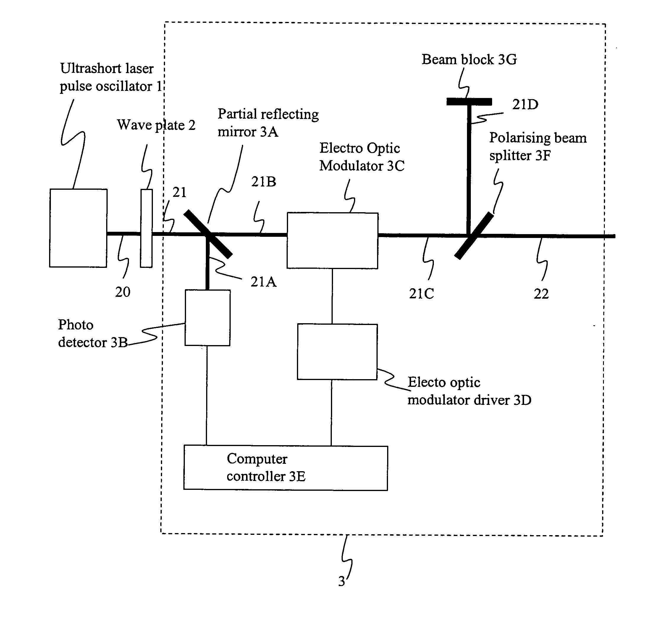
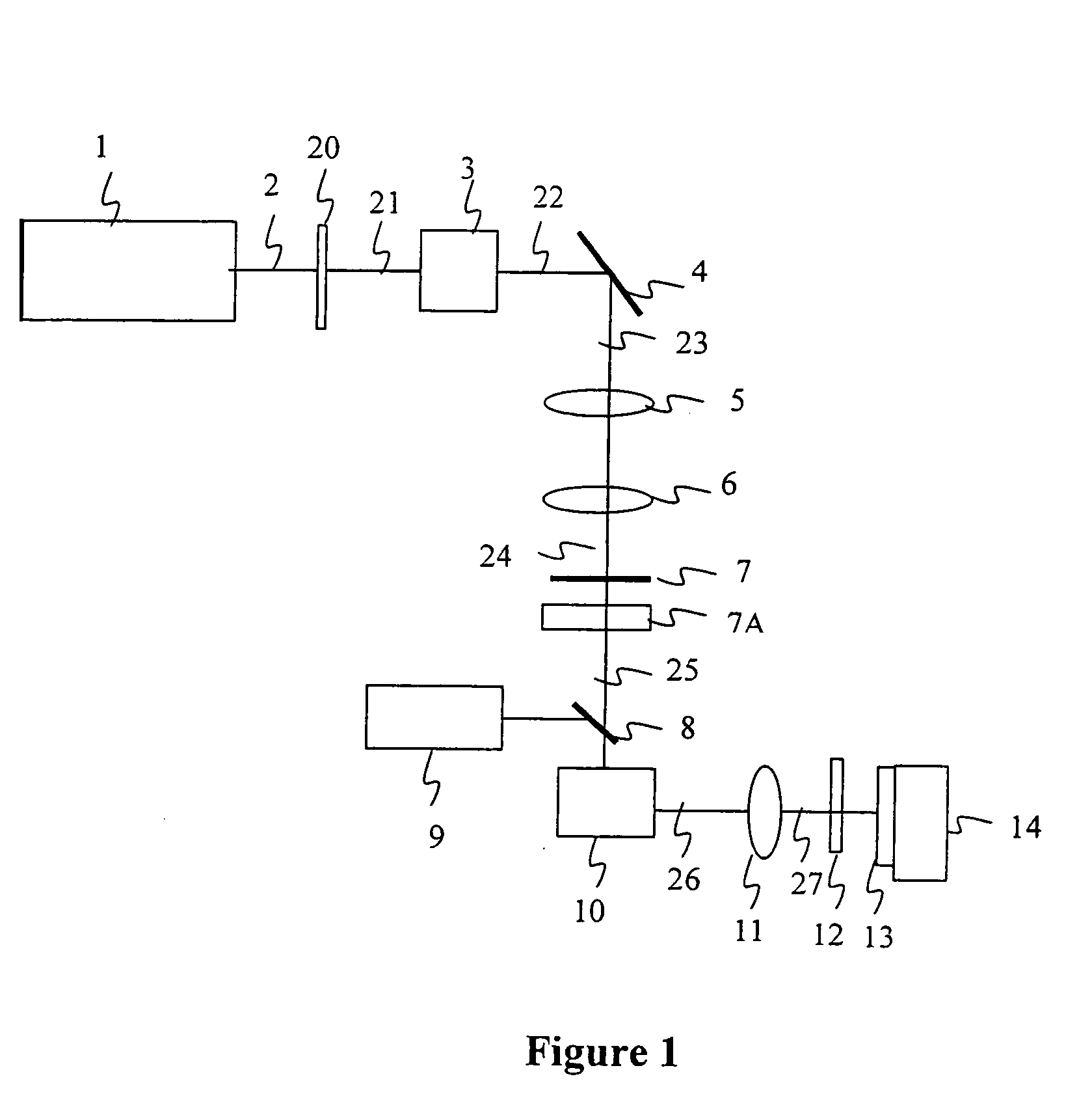
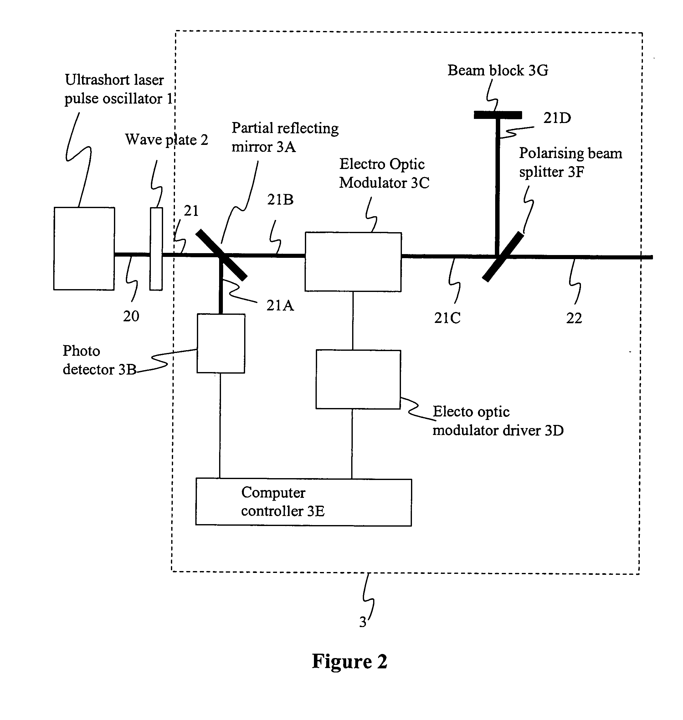
[0057] The object of the present invention is to provide an improved method and apparatus for dicing of thin and ultrathin semiconductor wafer and to ameliorate the aforesaid deficiencies of the prior art by using ultrafast pulse generated directly from the laser oscillator. The laser oscillators are mode locked diode pumped solid state laser system, which is stable and compact. The pulse laser beam having a pulse width of ifs to 100 ps of repletion rate from 1 MHz to 400 MHz is controlled by an electro optic modulator or acousto optic modulator. Alternatively, an amplified ultrafast laser source is used for dicing a semiconductor wafer of a thickness above 80 micrometer.

[0058] The modulated pulse is expanded to a required beam diameter by using a combination of positive and negative lens to act as a telescope. Varying the diameter of the laser beam, the focused laser spot size can be varied. The pulsed laser beam is scanned by a two axis galvanometer scanner to scan the pulse lase...


PUM

PropertyMeasurementUnit
Lengthaaaaaaaaaa
Lengthaaaaaaaaaa
Lengthaaaaaaaaaa

Abstract

The present invention relates to the apparatus, system and method for dicing of semiconductor wafers using an ultrafast laser pulse of femtosecond and picosecond pulse widths directly from the ultrafast laser oscillator without an amplifier. Thin and ultrathin simiconductor wafers below 250 micrometer thickness, are diced using diode pumped, solid state mode locked ultrafast laser pulses from oscillator without amplification. The invention disclosed has means to avoid/reduce the cumulative heating effect and to avoid machine quality degrading in multi shot ablation. Also the disclosed invention provides means to change the polarization state of the laser beam to reduce the focused spot size, and improve the machining efficiency and quality. The disclosed invention provides a cost effective and stable system for high volume manufacturing applications. An ultrafast laser oscillator can be a called as femtosecond laser oscillator or a picosecond laser oscillator depending on the pulse width of the laser beam generated.

Description

[0001] This Nonprovisional application claims priority under 35 U.S.C. § 119(e) on U.S. Provisional Application No. 60 / 579,238 filed on Jun. 15, 2004, the entire contents of which is hereby incorporated by reference.BACKGROUND OF THE INVENTION [0002] 1. Field of the Invention [0003] The present invention relates to a method and apparatus for dicing of thin and ultra thin semiconductor wafers using ultrafast pulse laser, and more specifically it relates to an apparatus and method for dicing using ultrafast pulse laser directly from an oscillator without an amplifier, operating in picosecond and femtosecond pulse width modes. [0004] 2. Description of the Related Art Dicing of Thin and Ultra Thin Silicon Wafer [0005] The semiconductor industry is moving towards thin silicon in various fields. The bulk of the silicon plays no role in the performance of the circuit, and hence the semiconductor industry is moving toward thin silicon. The reasons include a desire to increase the density o...

Claims


Application Information

Patent Timeline
IPC IPC(8): B23K26/38B23K26/40B23K26/06
CPCB23K2201/40B23K26/0624B23K26/40B23K2203/50B23K2101/40B23K2103/50
Inventor DESHI, TAN
Owner LASERFACTURING
Why Eureka
Try Eureka