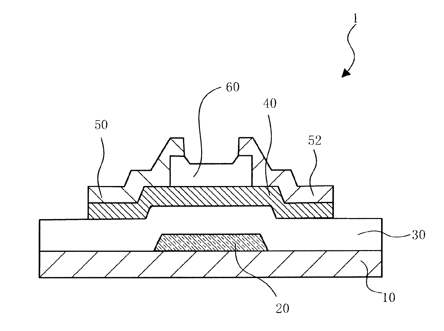
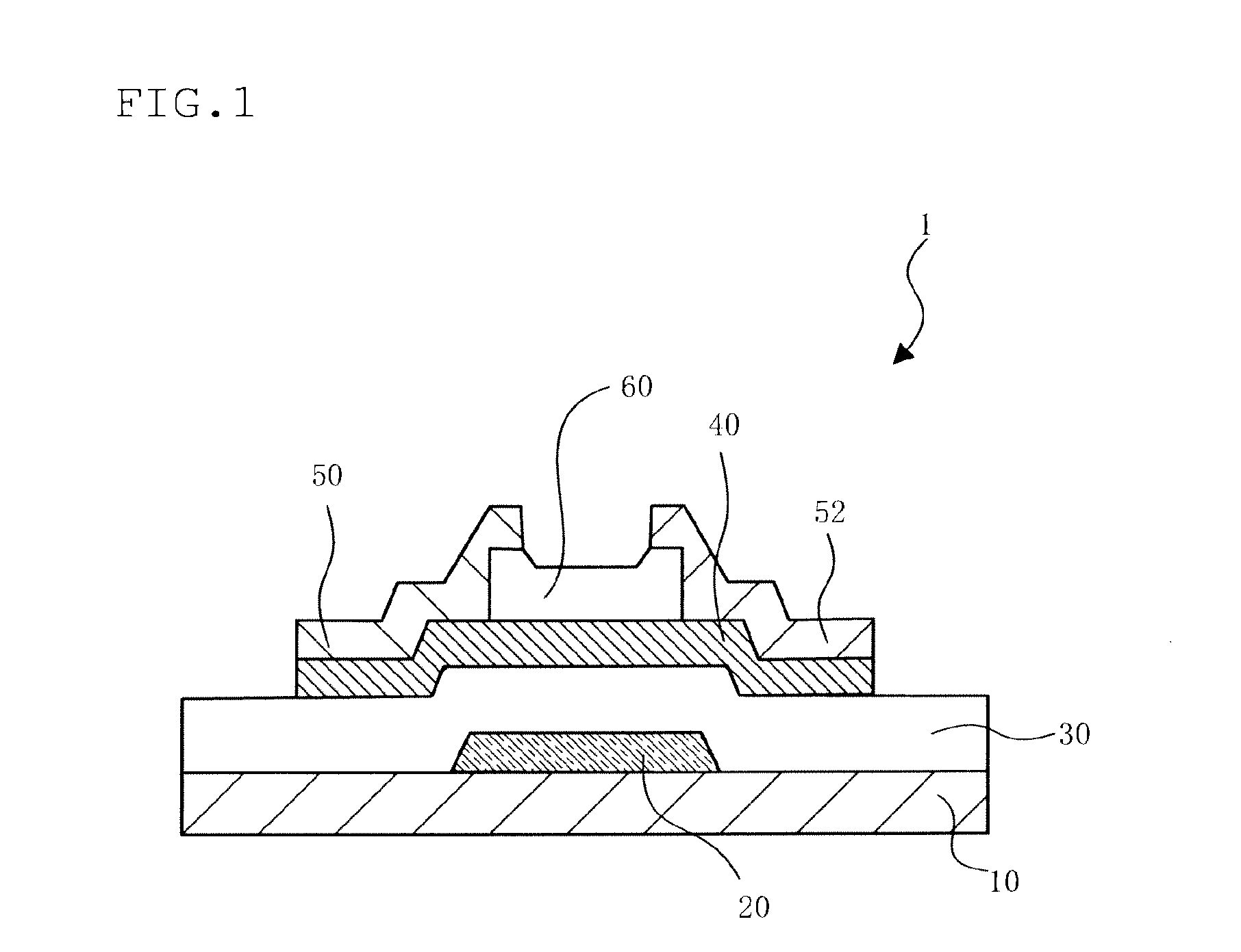
In-Ga-Sn OXIDE SINTER, TARGET, OXIDE SEMICONDUCTOR FILM, AND SEMICONDUCTOR ELEMENT
a technology of sputtering target and sintering body, which is applied in the direction of diaphragms, conductive materials, wood working apparatuses, etc., can solve the problems of low speed etching speed of amorphous oxide semiconductor films comprising zinc oxide, easy dissolved substances, and complex production processes and quality managemen
- Summary
- Abstract
- Description
- Claims
- Application Information
AI Technical Summary
Benefits of technology
Problems solved by technology
Method used
Image

Examples
example 1
(1) Preparation of an Oxide Sintered Body
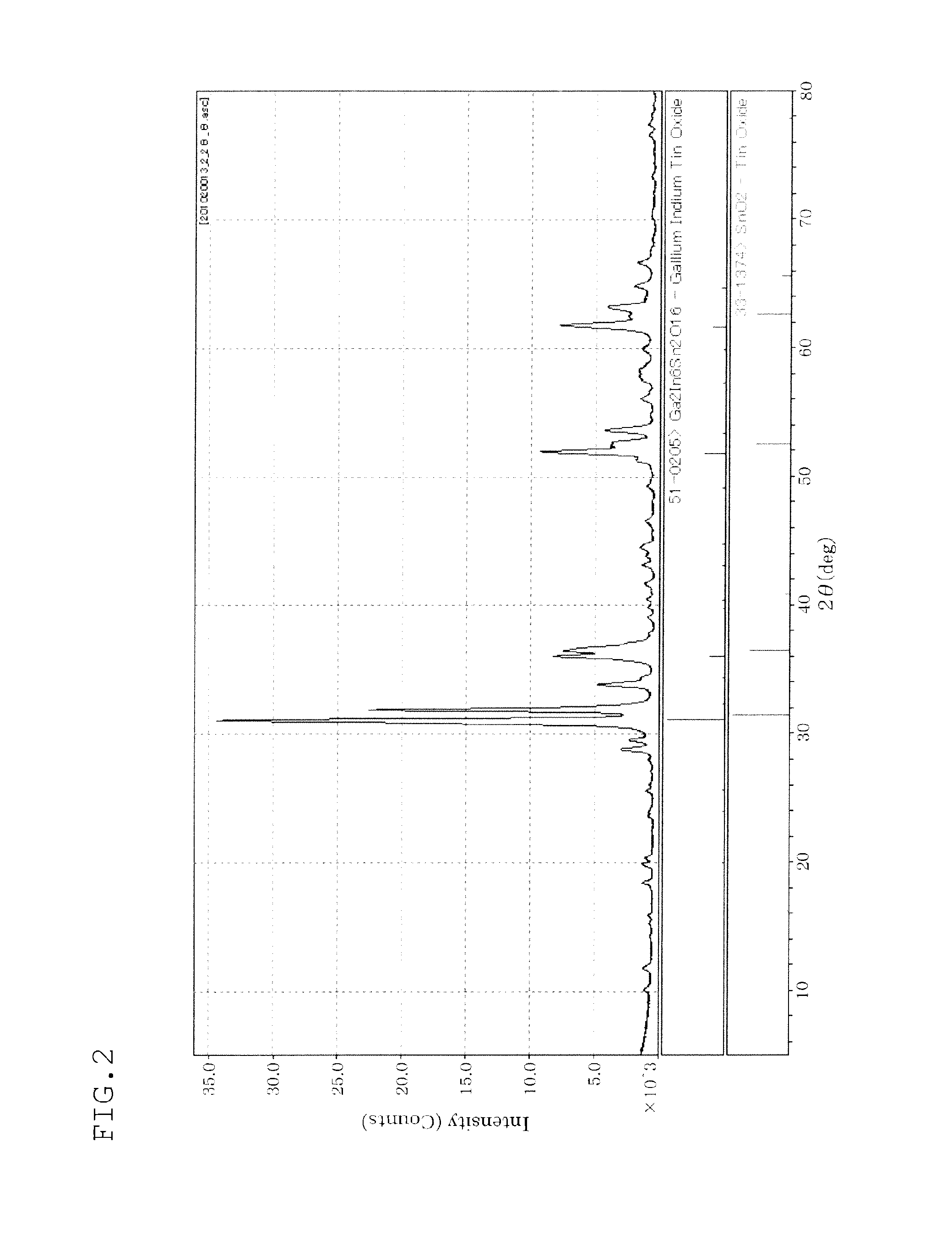
[0134]As a starting material, In2O3 (Purity 4N, BET surface area 15 m2 / g), Ga2O3 (Purity 4N, BET surface area 15 m2 / g) and SnO2 (Purity 4N, BET surface area 4 m2 / g) were used.
[0135]These raw materials were weighed such that the atomic ratio of the metal elements became the ratio of the oxide sintered body shown in Table 1, and mixed and pulverized by means of a ball mill.
[0136]After mixing and pulverizing, the mixture was dried by natural drying. The resulting mixture power was filled in a mold, and subjected to press molding by a pressing machine to prepare a shaped body having a thickness of 15 mm or more. At this time, the surface pressure was 400 kgf / cm2 and the retaining time was 2 minutes. Thereafter, pressing was conducted by CIP (cold isostatic pressing) under the conditions of a surface pressure of 2000 kgf / cm2 and a holding time of 5 minutes.
[0137]The resulting shaped body was sintered in a sintering furnace. Sintering was conducted...
examples 10 and 11
[0179]As the starting raw material, In2O3 (purity: 4N, BET specific surface area: 6 m2 / g), Ga2O3 (purity: 4N, BET specific surface area: 6 m2 / g) and SnO2 (purity: 4N, BET specific surface area: 6 m2 / g) were used.
[0180]These raw materials were weighed such that the atomic ratio of the metal elements became ratios shown in Table 2, and mixed by means of a super mixer. These raw materials were packed in an aluminum-made container, and subjected to pre-firing in the atmosphere of air at 950° C. for 5 hours. Subsequently, these raw materials were pulverized by means of an attritor (φ3 mm zirconia beads, agitator rotation speed 300 rpm) for about 0.5 to 5 hours. The slurry after the pulverization was dried by means of a spray dryer at 100 to 150° C. for 5 to 48 hours. The resultant was sieved by means of a sieve having an opening of 250 μm to collect the powder. The pulverization was conducted until the BET specific surface area became 10 m2 / g or more.
[0181]Subsequently, oxide sintered bo...
example 12
[0182]As the starting raw material, In2O3 (purity: 4N, median diameter: 1.8 μm), Ga2O3 (purity: 4N, median diameter: 1.8 μm) and SnO2 (purity: 4N, median diameter: 1.5 μm) were used. These raw materials were weighed such that the atomic ratio of the metal elements became ratios shown in Table 2.
[0183]These raw materials were pre-fired in the same manner as in Example 10, and then pulverized until the median diameter of the raw material mixture become 1.0 (pm). Subsequently, oxide sintered bodies or the like were produced and evaluated in the same manner as in Example 10.
PUM
| Property | Measurement | Unit |
|---|---|---|
| electron carrier density | aaaaa | aaaaa |
| electron carrier density | aaaaa | aaaaa |
| crystal structure | aaaaa | aaaaa |
Abstract
Description
Claims
Application Information