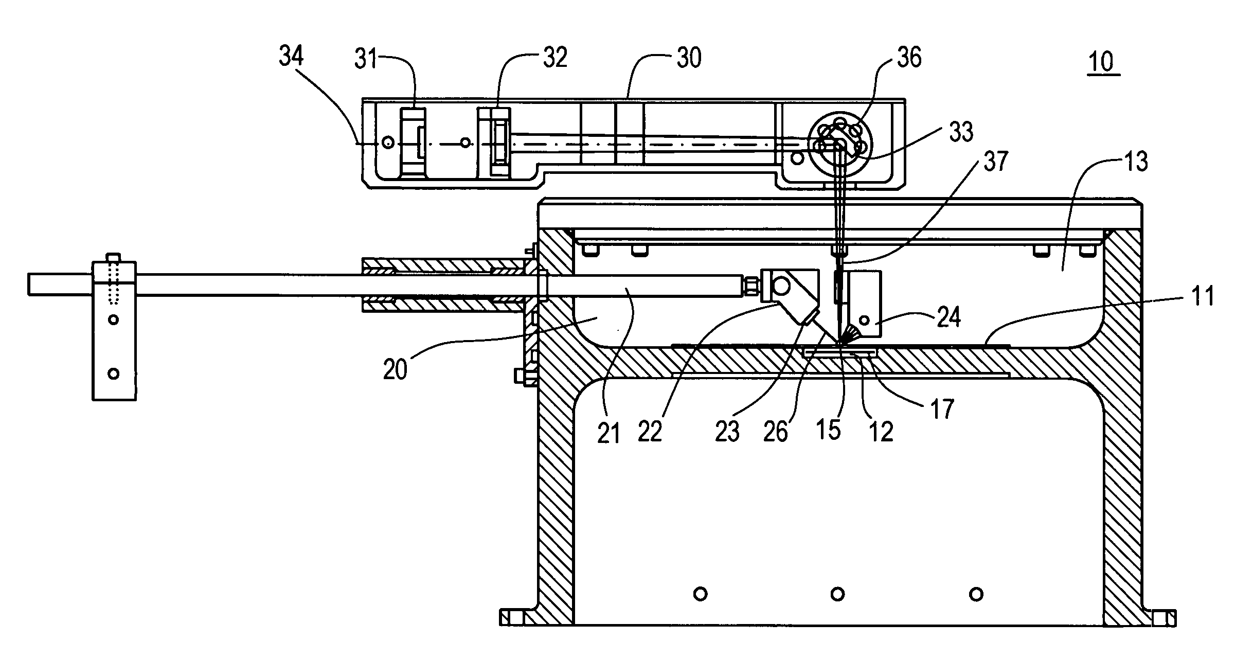
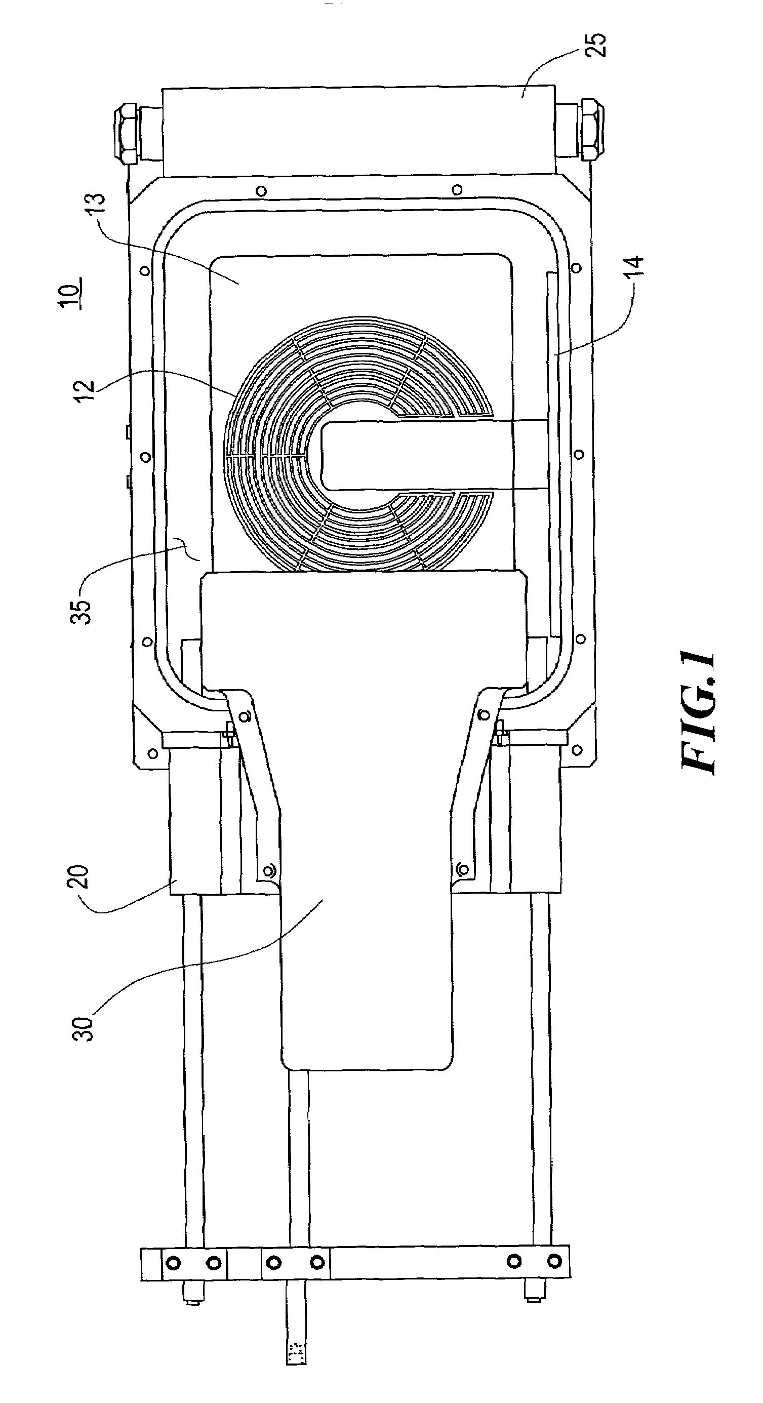
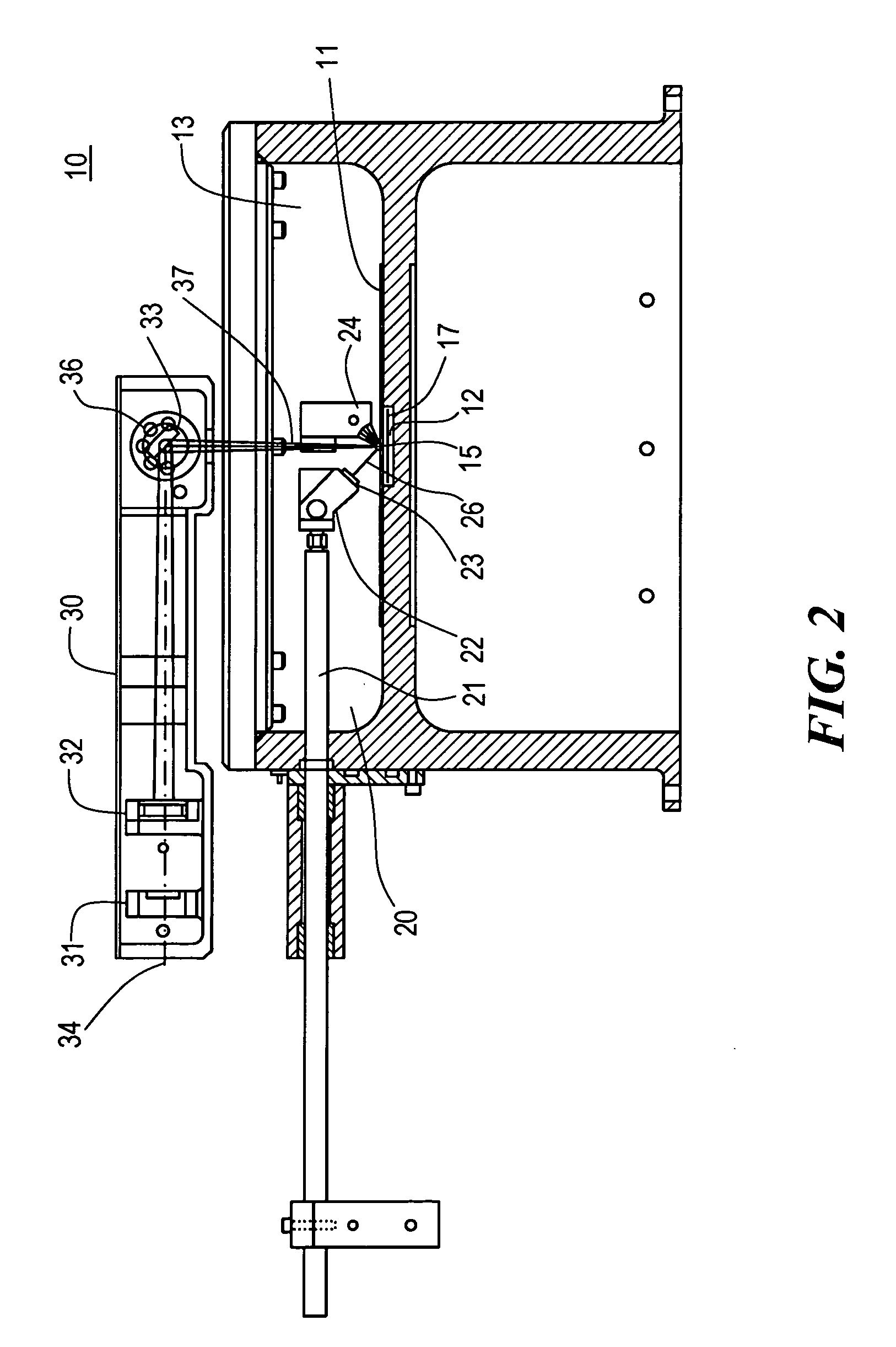
Scanning plasma reactor

a plasma reactor and plasma technology, applied in vacuum evaporation coatings, chemical vapor deposition coatings, coatings, etc., can solve the problems of large volume of gas and waste of energy required to excite large volume of gas, unwanted reactions on many surfaces, and large volume of interior volume filled, so as to reduce cycle time and equipment cost, reduce by-product contamination in the chamber, and high degree of reaction uniformity and process efficiency

Inactive Publication Date: 2007-09-18
NOVELLUS SYSTEMS
View PDF114 Cites 6 Cited by
  • Summary
  • Abstract
  • Description
  • Claims
  • Application Information

AI Technical Summary

Benefits of technology

[0012]It is a further object of this invention to provide such a plasma reactor which reduces or eliminates the problems of wafer and chamber contamination caused by the deposition of reaction by-products on the interior surfaces of the reactor vessel.
[0021]Since short wavelength UV radiation produces extremely high surface temperatures and reaction rates, the need to have high bulk temperature thermal processing is greatly reduced or eliminated.

Problems solved by technology

A fundamental problem with prior art reactors is that the interior volume is filled with gas and energy to drive the reaction, when only the wafer surface needs reacting.
This large volume of gas and the energy required to excite the large volume of gas is wasteful.
This causes unwanted reactions on many surfaces in addition to the substrate being processed.
There are six primary problems associated with prior art reaction chambers.
The first problem associated with prior art reaction chambers relates to the deposition of reaction products onto the reaction chamber surfaces.
During processing, gas reaction by-products form particles and residues on the chamber walls which, during subsequent processing, re-deposit onto the wafer, causing serious contamination and chip rejects.
One method to remove this contamination is to clean the chamber with nitrogen trifluoride (NF3), an expensive toxic gas; the cleaning procedure causes system downtime and reduces productivity.
The second problem associated with prior art reaction chambers relates to non-uniformity of the reactions taking place at the wafer surface.
A typical reaction chamber produces an energy field which is non-uniform, and also generates a gas distribution which is non-uniform.
The interactions of the energy and reactive gases are therefore non-uniform.
The result of reaction non-uniformity is variations in the thickness of deposited films, or non-uniform removal in etch reactions, or other deviations that impact the quality and yield of IC devices in manufacturing lines.
The third problem associated with prior art reaction chambers relates to their cost efficiency, measured in terms of gas consumption and wafer-per-hour productivity.
Since the activating energy and gas volume are not confined or specifically directed to the wafer surface, excess energy and gas is consumed, and excess process time is required to deposit or etch a film layer.
High cost of operation results from excess gas and energy consumption, and lower throughput or productivity results from excess process time.
The fourth problem relates to the use of vacuum environments in prior art reactors.
First, the time required to pull a vacuum and return to atmosphere causes productivity loss, since it represents a major portion of total process time.
Secondly, the equipment (big pumps, load locks, plumbing) required to provide vacuum environments is expensive and complex, thereby reducing both cost efficiency and reliability of the system.
Thirdly, the system size and footprint are increased to support deep vacuum processing, and space in IC fabrication clean rooms is extremely expensive.
The fifth problem relates to the use of many types of reactors to perform a variety of wafer surface processes, and the fact that they are not fully integrated.
This creates large capital expenses, as well as excess wafer handling from tool to tool; handling adds contamination to the wafer and lowers chip yield.
The sixth problem relates to the high thermal environment inside prior art reactors.
Wafers are subjected to high temperatures (800-1100° C.) in many reactors, which induce thermal stress, wafer warp, crystal plane slippage, dopant depth changes, and other undesirable effects.

Method used


Image

  • Scanning plasma reactor
  • Scanning plasma reactor
  • Scanning plasma reactor

Examples


example # 1

EXAMPLE #1

Copper Surface Modification

[0071]The UV irradiation of metallic copper will lead primarily to thermal heating for pulse durations on the nanosecond timescale, like those from an excimer laser. When copper films are placed over silicon dioxide, there is very poor thermal transfer to the silicon. This is partly because of the difference in atomic mass between copper and silicon and because there is effectively an interfacial layer at the junction of the two films. When thin copper films are therefore exposed with the scanning plasma reactor, about 68% of the UV radiation is retained within the copper layer, and the balance is reflected. Copper reflects ˜33% of 193 nm radiation; at 157 nm UV laser wavelengths, only 21% is reflected, e.g. more efficient heating. This would result in a temperature rise at the surface to 580° C., or sufficient heat to cause dramatic surface re-arrangement. This is useful in changing the grain structure of the metallic copper layer to enhance con...

example # 2

EXAMPLE #2

Growth of Shallow Junction Layers

[0082]The creation of a shallow but highly doped region of silicon is a common but critical step in the creation of modem IC chips. Control of the doping density and depth of the shallow junction is currently controlled by ion implantation followed by annealing for high quality circuits. The problem with ion implantation is that it generates significant and damaging heat to the bulk of the wafer, thereby requiring a separate annealing step to ‘anneal out’ the damage. It also converts photoresist layers which are typically present into disordered graphite, which can then only be removed by using a two step process: a microwave low temperature ashing to bum off the majority of the organic film, followed by a chemical step in a highly corrosive mixture of boiling sulfuric acid and hydrogen peroxide.

[0083]The scanning plasma reactor can be used to replace this process by simply depositing a thin layer of doped amorphous silicon on the surface o...

example # 3

EXAMPLE #3

Densification

[0088]Deposited thin layers may have microscopic voids that are undesirable and could detract from good performance. For example, the tungsten barrier layer that is used in copper-metalized IC chips needs to be free of cracks and voids. Rapid heating of this metal layer with a UV pulse could improve film quality and reduce defects by providing instantaneous heat and expansion at the film surface sufficient to close the microscopic voids, and thereby densify the layer.


PUM

PropertyMeasurementUnit
wavelength rangeaaaaaaaaaa
lengthaaaaaaaaaa
temperaturesaaaaaaaaaa

Abstract

A scanning plasma reactor for exciting reactant gases at a substrate surface including a beam forming module, a gas injection module, a reaction chamber with a window and a vacuum chuck, a gas exhaust module. Radiation from the beam forming module and the reactant gas create an excited plasma zone. The excited plasma zone is translated across the substrate like a windshield wiper blade, or the substrate is conveyed under a fixed gas reaction zone.

Description

FIELD OF THE INVENTION[0001]This invention relates to a UV-reactive gas plasma processing apparatus and method for film deposition, etching, doping, UV curing, melting, and other surface processing of a substrate(s), such as a wafer used in integrated circuit (IC) manufacturing.BACKROUND OF THE INVENTION[0002]The manufacturing of semiconductor devices and other small geometry electronic and optical devices, such as thin film heads , printed circuit boards, and compact discs, involves many surface processing operations. Examples of these surface processes include the following: deposition of a metal or dielectric layer onto a surface by energetic decomposition of an excited volume of gas; etching or removal of material from a surface in an excited gas plasma atmosphere; UV polymerization of a coating; crystallization or re-crystallization of a surface by exposure of the surface to a high temperature in an excited gas atmosphere; photochemical treatment of a surface to improve adhesio...

Claims


Application Information

Patent Timeline
Patent Type & Authority Patents(United States)
IPC IPC(8): H01L21/00C23C16/00C23C16/50H01J37/32
CPCC23C16/50H01J37/32321H01J37/32376
Inventor ELLIOTT, DAVID J.HARTE, KENNETH J.SHEPHARD, LARRY E.
Owner NOVELLUS SYSTEMS
Why Eureka
Try Eureka