[0067] It should be noted that in
flash memory chips, the convention has been to use the same floating
gate oxide that is used between the floating gate and the channel for the
gate oxide of low, and some medium
voltage transistors in order to save extra process steps. Therefore the conventional tunnel
oxide with a thickness that is usually greater than 8 nm has been limiting the performance, sub-threshold slope, and on-current drive of the low and some medium
voltage transistors. This has resulted in slower program, and read characteristics. One
advantage of the present invention is to provide a
peripheral transistor gate oxide that is electrically and effectively much thinner than the conventional tunnel
oxide, and is physically thicker than the conventional tunnel
oxide. In other words, the
peripheral circuitry will benefit from replacing the conventional tunnel oxide gate with high-K material(s) in alignment with the general trend of the
semiconductor industry towards high-K materials.
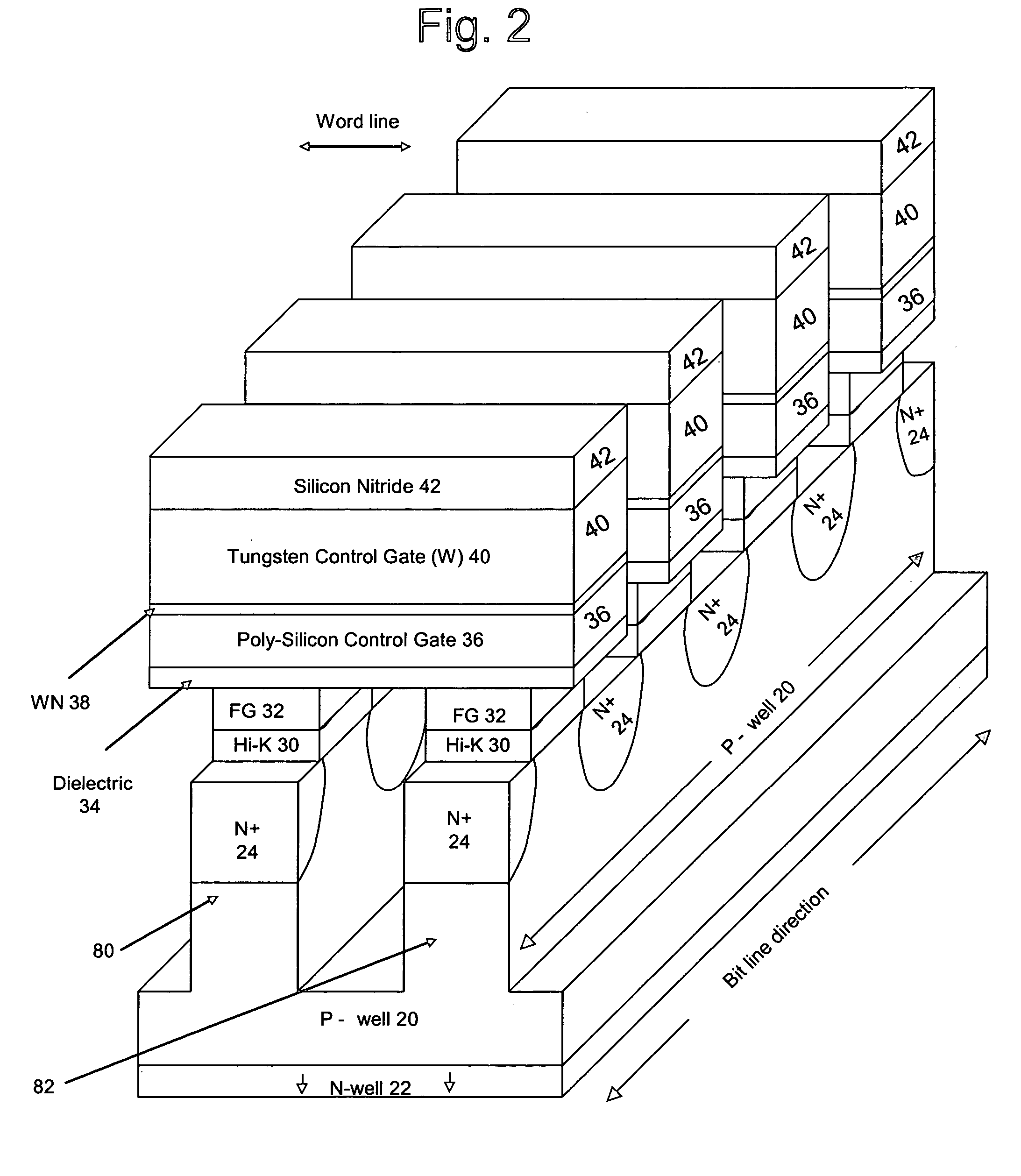
[0068] Step 402 of FIG. 9 includes performing implants and associated anneals of the triple well. The result of step 402 is depicted in FIG. 10A, which depicts P substrate 18, N-well 22 within P-substrate 18, and P-Well 20 within N-well 22. The sidewalls of the N-well that isolate the P-wells from one another are not depicted. Also the N-well depth is typically much thicker than that of the P-well in contrast to FIG. 10A. The P substrate is usually the thickest consisting of the majority of the
wafer thickness. In step 404, the high-K material(s) is deposited on top of P-Well 20. The high-K material may be deposited using
Chemical Vapor Deposition (CVD) including
Metal Organic CVD (MOCVD),
Physical Vapor Deposition (PVD),
Atomic Layer Deposition (ALD), or another suitable method. Additionally (and optionally), other materials may be deposited on, deposited under or incorporated within the high-K material in order to form
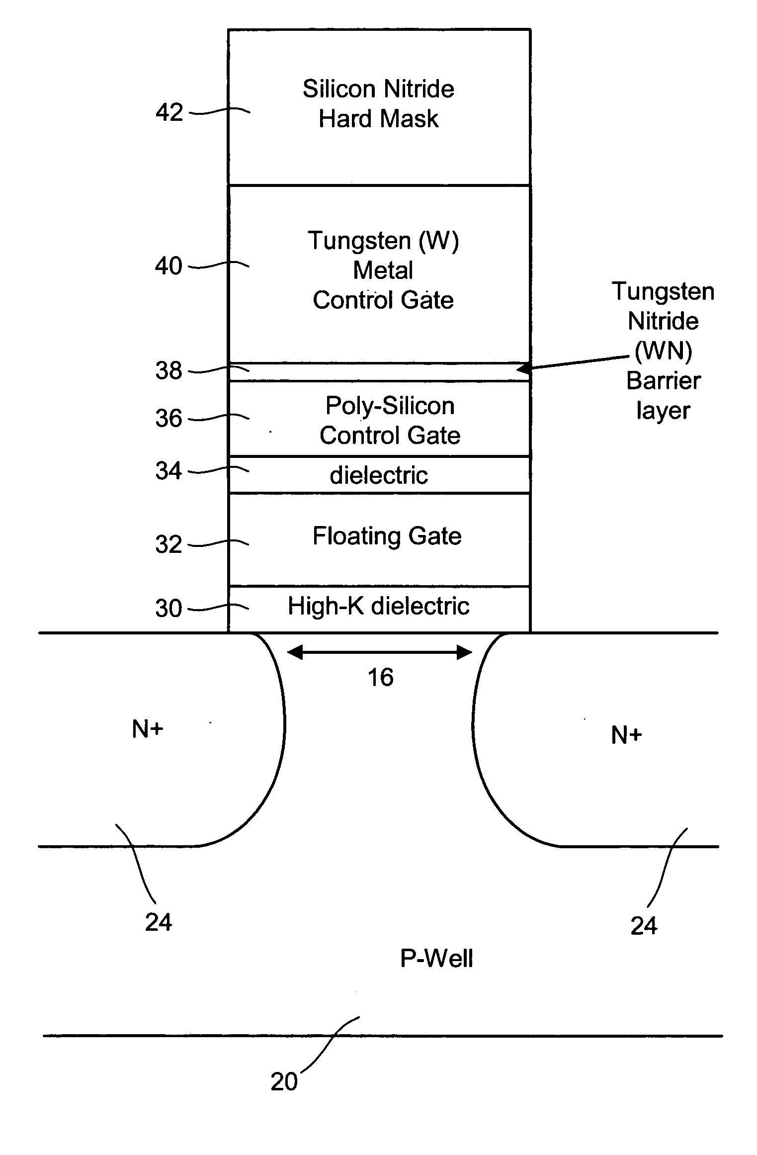
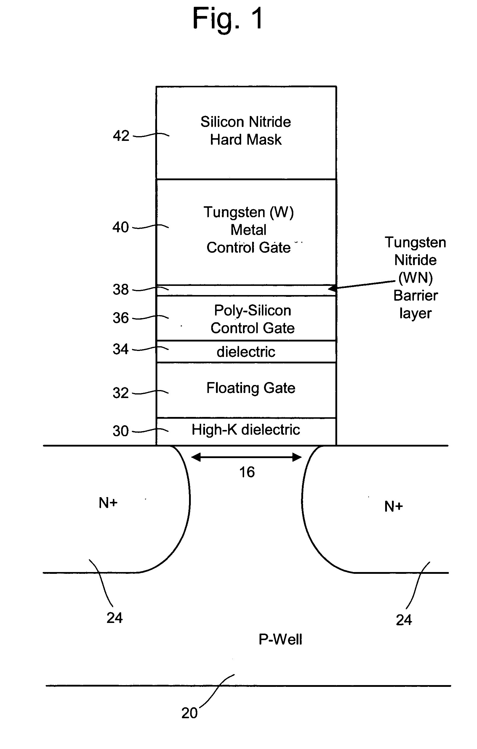
dielectric layer 30. The result of step 404 is depicted in FIG. 10B, which shows
dielectric layer 30, with the high-K material. Note that one
advantage of using the high-K material in the lower
dielectric layer is that it can also be used for
low voltage peripheral transistors to increase performance. In step 406, the floating gate is deposited over dielectric layer 30 using CVD, PVD, ALD or another suitable method. The result of step 402 is depicted in FIG. 10C, which shows floating gate layer 32 deposited on top of high-K dielectric layer 30.
[0069] Step 408 of FIG. 9 includes depositing a
hard mask using, for example, CVD, to deposit SiO2 or Si3N4. In step 410,
photolithography is used to form strips of
photoresist over what will become the NAND chains. Step 412 includes
etching through all
layers, including part of the substrate. First, the
hard mask is etched through using
anisotropic plasma etching, (i.e.
reactive ion etching with the proper balance between physical and chemical
etching for each planar layer encountered). After the
hard mask layer is etched into strips, the
photoresist can be stripped away and the hard
mask layer can be used as the
mask for etching the underlying
layers. The process, then includes etching through the floating gate material, the high-K dielectric material and approximately 0.1 micron into the substrate to create trenches between the NAND strings, where the bottom of the trenches are inside the top P-well 20. In step 414, the trenches are filled with SiO2 (or another suitable material) up to the top of the hard
mask using CVD, rapid ALD or PSZ STI fill as described in “Void Free and
Low Stress Shallow Trench Isolation Technology using P-SOG for sub 0.1 Device” by Jin-Hwa Heo, et. al. in 2002 Symposium on VLSI Technology Digest of Technical Papers, Session 14-1. PSZ STI fill is
Polysilazane Shallow trench isolation fill The fill sequence includes spin coat by coater, and densify by furnace. Si—N bond conversion to Si—O bond enables less shrinkage than conventional SOG (Spin On Glass). Steam oxidation is effective for efficient conversion. One proposal is to use Spin-On-Glass (SOG) for the dielectric layer, which is called
polysilazane-based SOG (SZ-SOG), a material used in integrating the
inter layer dielectric (ILD) applications because of its excellent
gap filling and planarization properties, and
thermal oxide like film qualities.
[0070] In step 416 Chemical Mechanical
Polishing (CMP), or another suitable process, is used to polish the material flat until reaching the floating gate poly-
silicon. The floating gate is polished to 20 nm (10-100 nm in other embodiments). In step 418, the inter-poly tunnel dielectric (e.g. dielectric 34) is grown or deposited using ALD, CVD, PVD, Jet Vapor Deposition (JVD) or another suitable process. FIG. 10D, which shows the inter-poly dielectric region 34 over floating gate 32, depicts the device after step 418. Examples of materials that can be used for the inter-poly tunnel dielectric include (but are not limited to) SiO2, Si3N4, an
alloy with a varying
mole fraction as a function of depth, an
alloy or nano-laminate of aluminum oxide and
silicon oxide, an
alloy or nano-laminate of
silicon nitride and
silicon oxide, an alloy or nano-laminate of
silicon oxide and
hafnium oxide, an alloy or nano-laminate of aluminum oxide and
hafnium oxide, or other suitable materials.
[0071] In one embodiment, the inter-poly tunnel oxide layer can be created in the manner disclosed by “Resonant Fowler-Nordheim Tunneling through Layered Tunnel Barriers and its Possible Applications,” Alexander Korotkov and Konstantin Likharev, 1999 IEEE, 0-7803-5413-3 / 99 (hereinafter “Likharev I”); “Riding the Crest of a New Wave in Memory, NOVORAM: A new Concept for Fast, Bit-Addressable Nonvolatile Memory Based on Crested Barriers,” Konstantin and Likharev, Circuits and Devices, July 2000, p. 17 (hereinafter “Likharev II”); or U.S. Pat. No. 6,121,654 granted Sep. 19, 2000 titled: “Memory device having a crested
tunnel barrier” all of which are incorporated herein by reference in their entirety. The oxide layer bottom of the
conduction band energy diagram can be rounded near the mid-depth region of the tunnel dielectric, instead of forming a sharp triangle as in FIG. 3a of U.S. Pat. No. 6,121,654, which is incorporated herein by reference in its entirety, by varying the
mole fraction of binary oxides such as (HfO2)x(Al2O3)1-X
Atomic layer deposition (ALD) can be employed to deposit mixed multiple dielectrics (e.g. (HfO2)x(Al2O3)1-x) (see “Energy gap and band alignment for—(HfO2)x(Al2O3)1-x on—100-Si” by H. Y. Yu et. al. Applied
Physics Letters Volume 81, Number 28, July 2002 (“hereinafter “Yu”)), whose
mole fraction, x, gradually changes with depth into the oxide in order to create crested barriers (see Likharev I and Likharev II) that not only facilitate tunneling at lower voltages but also improve
retention time and reduce disturb problems. Also
Hafnium oxide and
Silicon oxide, or Aluminum oxide and
Silicon oxide can be paired to create crested
conduction band edges. There are probably many more ALD deposited material systems composed of 2 or more materials that can have their
conduction band edge
energy level change in a linear or non-linear manner with changing depth in order to optimize the conduction
band engineering of the tunnel dielectric. Switching of
chemistry of ALD deposited tunnel barriers after every
single cycle or after every few cycles of deposition can create the gradual change of mole fraction that may be conducive to constructing a tunnel dielectric that does not suffer from the issues arising from having material interfaces within the tunnel dielectric, such as
trapping at mentioned interfaces. An anneal of proper duration and temperature may further smooth the changing of mole fraction. For a crested barrier, the mole fraction x has to smaller near the interfaces and gradually peak at the middle of the barrier).
[0072] In step 440 of FIG. 9, which is an optional step, the inter-poly tunnel oxide is annealed to densify the oxide, without damaging the high-K materials due to a high temperature. Note that Al2O3 will crystallize at approximately 800 degrees Celsius, HfO2 will crystallize at approximately 500 degrees Celsius, HfSiOx will crystallize at approximately 1100 degrees Celsius, and HfSiON will crystallize at approximately 1300 degrees Celsius. In general, longer
exposure times to high temperatures will result in reduced
crystallization temperatures. Some of the most reliable tunnel oxides are grown
Silicon Oxi-
Nitride, grown
Silicon Oxide, and low temperature grown oxide by
Oxygen Radical generation in
high density Krypton plasma at temperatures as low as 400 degrees Celsius. In step 444, the one or more
layers of the control gate are deposited on the inter-poly tunnel oxide. In one embodiment, the materials deposited during step 444 include poly-silicon (e.g. layer 36), while in other embodiments this layer may be a
metal layer with a proper
work function,
thermal stability, and etch characteristics. In some embodiments, the control gate is composed of the poly-silicon layer 36,
tungsten-
nitride layer 38, and
tungsten layer 40, all of which are deposited in step 444.
Nitride layer 38 and
tungsten layer 40 are deposited to reduce the control gate
sheet resistance and form lower resistivity word lines. These materials can be deposited in a
blanket form using CVD, ALD, PVD or other suitable process. FIG. 10E, which shows polysilicon control gate 36, WN layer 38 and
Tungsten metal layer 40 over inter-poly tunnel oxide 34, depicts the device after step444.

