
Ferroelectric ceramic compound, a ferroelectric ceramic single crystal, and preparation processes thereof

a technology of ferroelectric ceramic and compound, which is applied in the direction of niobium compounds, lead oxides, device material selection, etc., can solve the problems of single crystal not being commercialized heretofore, difficult to grow to a commercially applicable single crystal having a diameter of 5 cm (2 inches) or greater, and achieve low dielectric loss, improve the uniformity of inside temperature, and high non-linearity of permittivity

Active Publication Date: 2006-09-28
IBULE PHOTONICS
View PDF6 Cites 5 Cited by
  • Summary
  • Abstract
  • Description
  • Claims
  • Application Information

AI Technical Summary

Benefits of technology

[0012] Particularly, an object of the present invention is to provide a process of preparing a ceramic composition having superior electrical and physical properties and a homogeneous single crystal using the same, which comprises a high-temperature calcination step that is called an [L] reaction step, and an additive addition step if the control of properties including a temperature property is required in the reaction step, in order to improve uniformity of the composition of components and expand a use range thereof.
[0026] The ceramic precursor reaction step is the step of mixing 0.09 to 0.20 mol, 0.09 to 0.20 mol and 0.01 to 0.27 mol of magnesium oxide (MgO) or zinc oxide (ZnO), niobium oxide (Nb2O5), and titanium dioxide (TiO2), respectively, with one another, adding one or more metals selected from the group consisting of lithium tantalate (LiTaO3), lithium niobate (LiNbO3), lithium (Li) or lithium carbonate (Li2CO3), platinum (Pt), gold (Au), silver (Ag), palladium (Pd), rhodium (Rh), indium (In), nickel (Ni), cobalt (Co), iron (Fe), strontium (Sr), scandium (Sc), ruthenium (Ru), copper (Cu), yttrium (Y) and ytterbium (Yb), or oxides thereof as additives for facilitating a reaction or controlling properties, and causing them to react with one another at a high temperature of 1,100 to 2,000° C.
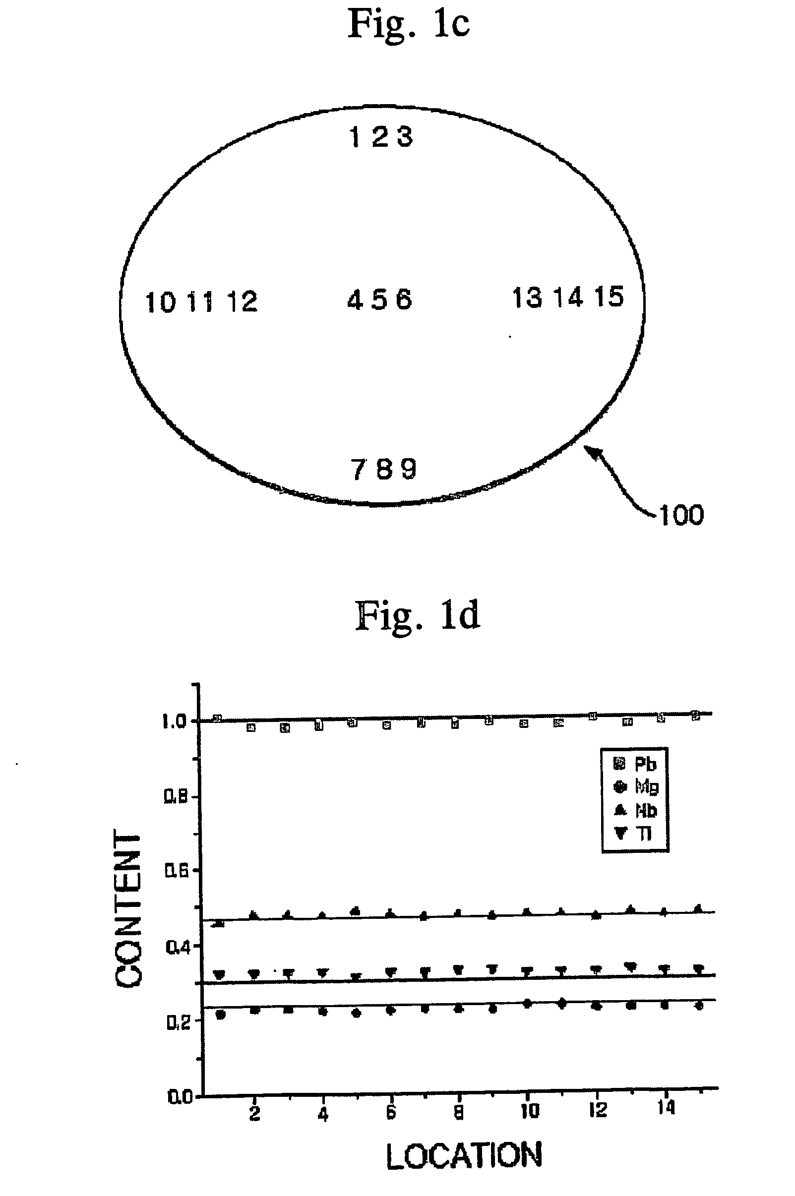
[0030] A ferroelectric single crystal of the present invention is prepared through the first solid phase reaction step at a high temperature that is called the [L] reaction step as the precursor reaction step, the second solid phase reaction step that is a complete ceramic composition reaction step, and the melting-crystallization step of the resultant ceramic compound. The single crystal prepared in such a manner is a novel, homogeneous material. The single crystal has an electromechanical coupling coefficient and piezoelectricity higher than those of single crystals that have been reported heretofore, light transmittance of 60% or greater, a high electrooptical coefficient, and high composition uniformity in a mass of the single crystal or respective regions of a wafer. Thus, the single crystal of the present invention can be usefully employed in ultrasonic transducers, devices for radio communication, optical modulators that are functional devices for optical communication, nonvolatile memory devices and actuators for micro-displacement control.
[0033] One of lead oxides (PbxOy) belonging to the [P] group is selected and mixed with the mixture obtained above. Then, the resultant mixture is pulverized, mixed, dried and calcined by means of the aforementioned process. Here, the calcination for the second reaction may be performed, for example, for 1 to 10 hours at a temperature of 800 to 1,000° C. The ceramic powder having the novel composition obtained in the above way is a novel ferroelectric ceramic compound having superior temperature property and high composition uniformity.
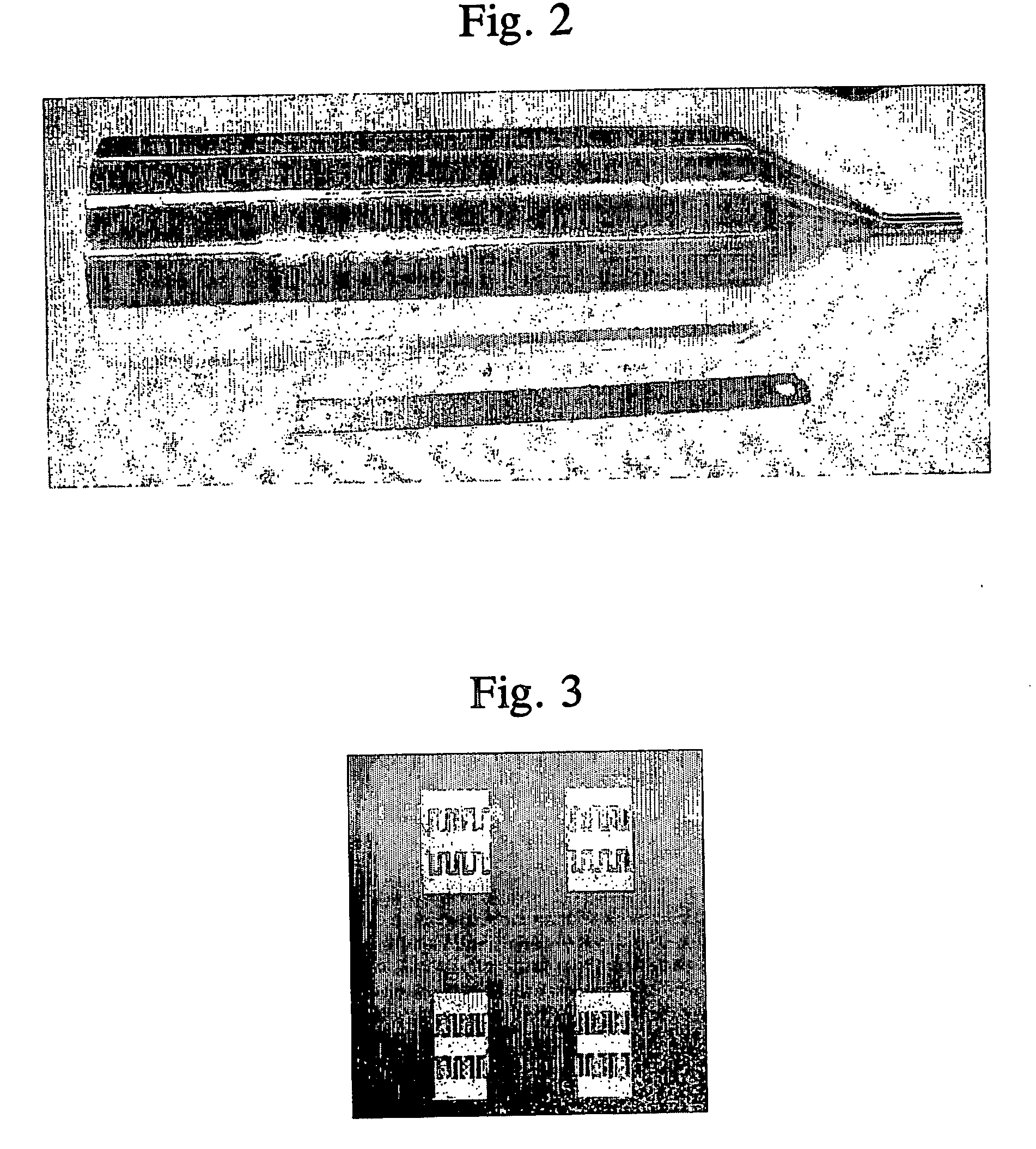
[0035] In the melting-crystallization step, the ceramic compound that has been subjected to the [L] reaction and the second solid phase reaction is melt in a platinum crucible, a platinum-rhodium alloy crucible, an iridium crucible, a zirconium crucible or a ceramic crucible, which has a diameter of 5 cm or greater as shown in FIG. 2, under high temperature and pressure, and the melt is then slowly cooled to be crystallized. The melting is performed in a closed crucible under a high temperature of 1,200 to 1,500° C. and a high pressure of 10 to 1,000 psi. Then, the melt is maintained at the high temperature for 360 to 500 hours and slowly cooled to room temperature for about 80 to 100 hours. With this step, the material is formed to be homogeneous in the level of atoms or molecules and a lattice structure. Therefore, it is possible to obtain a single crystal having a homogeneous composition that exhibits physical and chemical properties completely different from those of the ceramic compound obtained after the ceramic composition reaction step. Further, since the diameter of the crucible can be freely increased, it is possible to prepare a circular single crystal having as large a diameter as required. Generally, the diameter of the single crystal can be increased to 30 cm. However, in the case where the diameter of the single crystal is increased, it is preferred that the crucible be rotated or provided with a particular cooling device to improve the uniformity of inside temperature and its composition.
[0036] Meanwhile, typical ferroelectric materials include barium strontium titanate (BST), strontium titanate (STO) and the like. However, they are prepared in the form of a film due to difficulty in preparing them in the form of a single crystal. There are advantages in that these materials have low dielectric loss and high non-linearity of permittivity even at a high frequency (several tens GHz). However, there are disadvantages in that material properties greatly vary according to preparation processes of a film and a high electric field should be applied to obtain a sufficient rate of change in capacitance. If the materials are prepared in the form of the single crystal in accordance with the present invention, there are advantages in that the properties are stably maintained, it is possible to obtain high permittivity higher than that of BST, and a high rate of change in capacitance is obtained even in a low electric field.

Problems solved by technology

The term “relaxor” means the property of relaxing temperature dependency by which physical property values are affected by outside temperature, which is a critical problem that most electrical parts or devices, materials, equipment and the like have.
However, the single crystal that has superior properties and is expected to be applied to various latest devices as described above is generally very difficult to grow to a commercially applicable single crystal having a diameter of 5 cm (2 inches) or greater.
Thus, the single crystal has not yet been commercialized heretofore.
Therefore, the development of a device using such a single crystal has not been made.
Thus, there is a disadvantage in that the method cannot be used for commercial mass production.
The major reason that such a relaxor ferroelectric single crystal has not yet been applied to commercial devices though studies on the relaxor ferroelectric single crystal have been continuously conducted for last 40 years is that it is impossible to stably produce a large single crystal having a diameter of about 5 cm by using the existing single crystal growth method, in view of the properties of the ferroelectric material containing a great deal of lead component.
However, the methods also have problems in that composition uniformity is deteriorated in a single crystal due to a low phase-transition temperature, and its application range is relatively narrow.

Method used


Image

  • Ferroelectric ceramic compound, a ferroelectric ceramic single crystal, and preparation processes thereof
  • Ferroelectric ceramic compound, a ferroelectric ceramic single crystal, and preparation processes thereof
  • Ferroelectric ceramic compound, a ferroelectric ceramic single crystal, and preparation processes thereof

Examples


example

Ferroelectric Ceramic Compound and Preparation of a Single Crystal Thereof

[0046] Raw materials in the [L] reaction step listed in Table 1 below, which shows components of a ferroelectric single crystal of the present invention, were measured and mixed. The mixture was pulverized and mixed using ethanol as a dispersion medium in a 0.5″ zirconia ball mill. Then, the resultant mixture was dried in an electric furnace controlled at the temperature of 150° C. The dried mixture was calcined in a capped alumina crucible with a lid at the temperature of 1,600° C. for 6 hours to complete the first reaction. The calcined material obtained this way was uniformly pulverized again by using the ball mill. The first resultant reactants obtained in the above way was subjected to the [P] composition step and then calcined in the capped alumina crucible at the temperature of 920° C. for 4 hours to complete the second reaction.

[0047] The obtained ceramic powder was charged into a platinum crucible t...

experiment 1

Test of Electromechanical and Piezoelectric Performance for Manufacturing a Medical Ultrasonic Diagnosis Apparatus

[0048] To measure properties necessary for fabrication of a transducer for an ultrasonic diagnosis apparatus using the single crystal obtained in the example, both sides of the single crystal was polished to have a thickness of 0.5 mm and then cleaned using a ultrasonic cleaner. Thereafter, chrome electrodes of 15 mm×5 mm were formed on the both sides by using a DC magnetron sputter (Model KVSC T5050, a product of Korea Vacuum Science).

[0049] The dielectric constant and dielectric loss of the single crystal were calculated based on capacitance and dissipation measured at 1 kHz and 0.5 Vrms using HP 4192A LF impedance analyzer (available from Hewlett-Packard Co.). Further, as for the piezoelectric property, an electric field of 4 kV / cm was applied to the single crystal at 120° C. for 30 minutes for crystal polarizing. Thereafter, the electromechanical coupling coefficie...

experiment 2

Fabrication and Test of a Variable Capacitor for use in Manufacturing Tunable Filters for Radio Communication

[0052] Two types of coplanar capacitor and interdigital capacitor (IDC) were used. An IDC structure formed on a single crystal substrate of the present invention shown in FIG. 3 has an advantage in that its capacitance can be increased if a strong electric field is applied thereto by reducing the spacing between electrodes. However, the IDC structure has a disadvantage in that it is modeled as a complex equivalent circuit. A surface of a substrate using the piezoelectric single crystal prepared in the example was subjected to ultrasonic cleaning at 40° C. for 20 minutes in a solution comprising 5% of DECONEX and 95% of deionized water that is widely used for removing organics, rinsed and cleaned again by a conventional semiconductor surface cleaning process.

[0053] On the cleaned surface of the single crystal, an aluminum alloy (Al-0.5%Cu) was deposited at a thickness of abo...


PUM


Abstract

The present invention relates to a ferroelectric ceramic compound having the composition of the following formula: s[L]-x[P]y[M]z[N]p[T], a ferroelectric ceramic single crystal, and preparation processes thereof. The ferroelectric ceramic compound and the single crystal according to the present invention are relaxor ferroelectrics having high piezoelectricity, a high electromechanical coefficient and a high electrooptical coefficient, and are useful for manufacturing tunable filters for radio communication, optical communication devices, surface acoustic wave devices, and the like. Particularly, the process of preparing the single crystal according to the present invention enables preparation of a single crystal having a diameter of 5 cm or greater and a single crystal wafer with uniform composition. In the formula, [P] is lead oxide, [M] is magnesium oxide or zinc oxide, [N] is niobium oxide, [T] is titanium oxide, [L] is one selected from the group consisting of lithium tantalate or lithium niobate, lithium, lithium oxide, platinum, indium, palladium, rhodium, nickel, cobalt, iron, strontium, scandium, ruthenium, copper, yttrium, and ytterbium or mixtures thereof, and x, y, z, p and s are defined as 0.55<x<0.60, 0.09<y<0.20, 0.09<z<0.20, 0.01<p<0.27 and 0.01<s<0.1, respectively.

Description

TECHNICAL FIELD [0001] The present invention relates to a ferroelectric ceramic compound, a ferroelectric ceramic single crystal, and preparation processes thereof. More particularly, the present invention relates to a widely applicable ferroelectric ceramic compound having superior ferroelectric, piezoelectric, electromechanical, electrooptical, and electrostrictive properties, a single crystal having a diameter of 5 cm or greater prepared therefrom, and preparation processes thereof. BACKGROUND ART [0002] A single crystal means a homogeneous material having one regular arrangement without any boundaries, contrary to materials in which general ceramic components exist in the form of powder and particles thereof disorderly exist in a state where the particles have boundaries. Due to such a regular physical state, the single crystal provides physical, electromechanical, optical and electrooptical properties completely different from those of general ceramics and thus is used for prep...

Claims


Application Information

Patent Timeline
IPC IPC(8): E04B1/74C01G21/02C01G33/00C30B11/00C30B29/22H01G7/06H01L21/314H01L21/316H10N30/85
CPCC01G33/006C01P2006/40C30B11/00C30B29/22H01G7/06H01L21/3147H01L21/31691H01L41/18H01L21/02266H01L21/02271H01L21/02197H10N30/85C01G21/02
Inventor LEE, SANG-GOOKIM, MIN-CHANCHOI, BYUNG-JUSHIN, MIN-CHULYU, SU-HAN
Owner IBULE PHOTONICS
Learn More