Semiconductor structure

a semiconductor structure and semiconductor technology, applied in the direction of semiconductor/solid-state device details, transistors, coatings, etc., can solve the problems of hard control of crystal grain size, disadvantages of metals having amorphous structures, generation of joule heat or delay, etc., and achieve the effect of reducing device size and high step coverag

Inactive Publication Date: 2009-05-28
NAT INST OF ADVANCED IND SCI & TECH
View PDF21 Cites 25 Cited by
  • Summary
  • Abstract
  • Description
  • Claims
  • Application Information

AI Technical Summary

Benefits of technology

[0015]In consideration of the above, one of the desired properties for the metal gate electrode layer, which can realize reduction of a device size further to existing semiconductor devices having polysilicon electrodes, is that it is depositable on a three-dimensional semiconductor structure having a microstructure with high step coverage. Another desired property for the metal gate electrode layer is that a surface of a deposited electrode layer is flat on a nanometer scale, so that a dielectric lay

Problems solved by technology

Therefore, the metal having an amorphous structure has a disadvantage from the viewpoint of generation of Joule heat or delay when applied to semiconductor devices.
However, although generally inferior to a single-crystal metal, the metal having an amorphous structure has excellent flatness of surface and homogeneity of electric characteristics compared with a polycrystalline material having many crystal grain

Method used


Image

  • Semiconductor structure
  • Semiconductor structure
  • Semiconductor structure

Examples


embodiment 1

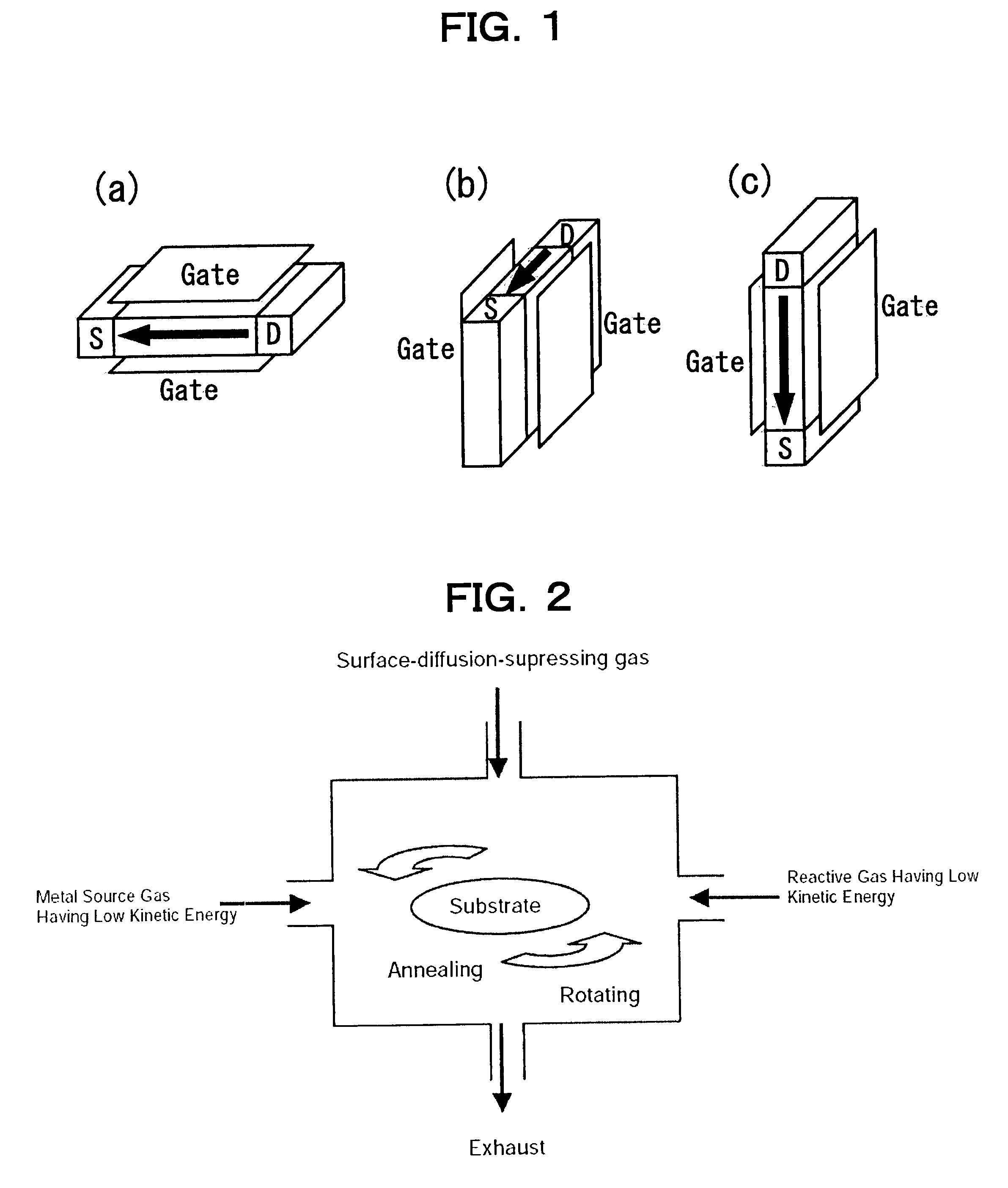
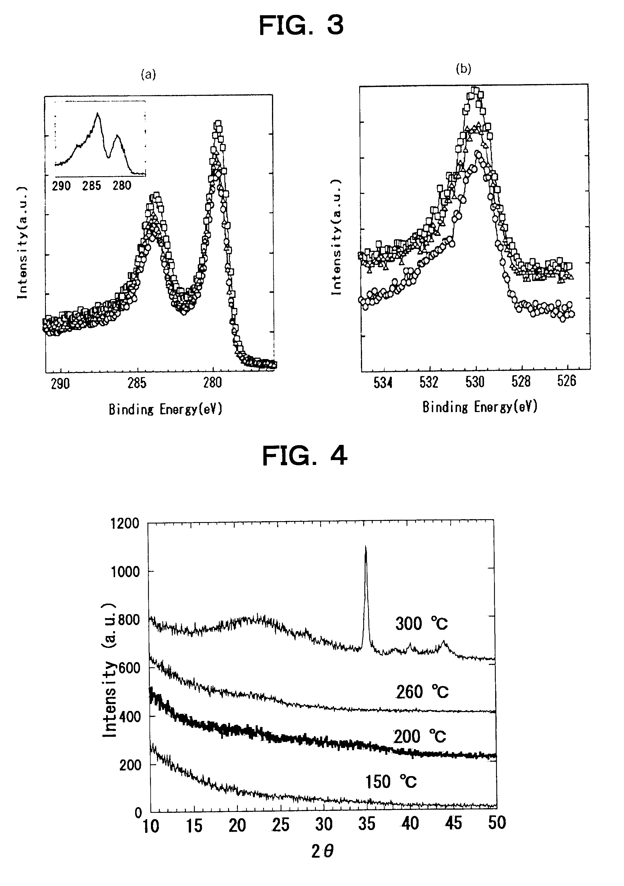
[0057]As amorphous compound metals, a Ru oxide was selected. RuO2 is an example of a Ru oxide and has a rutile structure and exists as a compound metal. RuO2 is already known as a material for electrodes using high-dielectric oxide and has been used in capacitors for DRAMs or in ferroelectric memories. All Ru oxide electrodes currently used, however, are polycrystalline materials and diffusion of impurity atoms along crystal grain boundaries occurs. Therefore, for example, in order to prevent diffusion of Pb atoms in a PZT ferroelectric body or diffusion of oxygen atoms from diffusing into a metal underlayer, a barrier metal such as TiN or TaN is required. If an amorphous Ru oxide electrode can be realized, such diffusion of impurity through grain boundaries could be suppressed thereby and the amorphous Ru oxide electrode may also be used as the barrier metal. Thus, according to the present invention, formation of an amorphous Ru oxide was attempted.

[0058]FIG. 2 shows a schematic vi...

embodiment 2

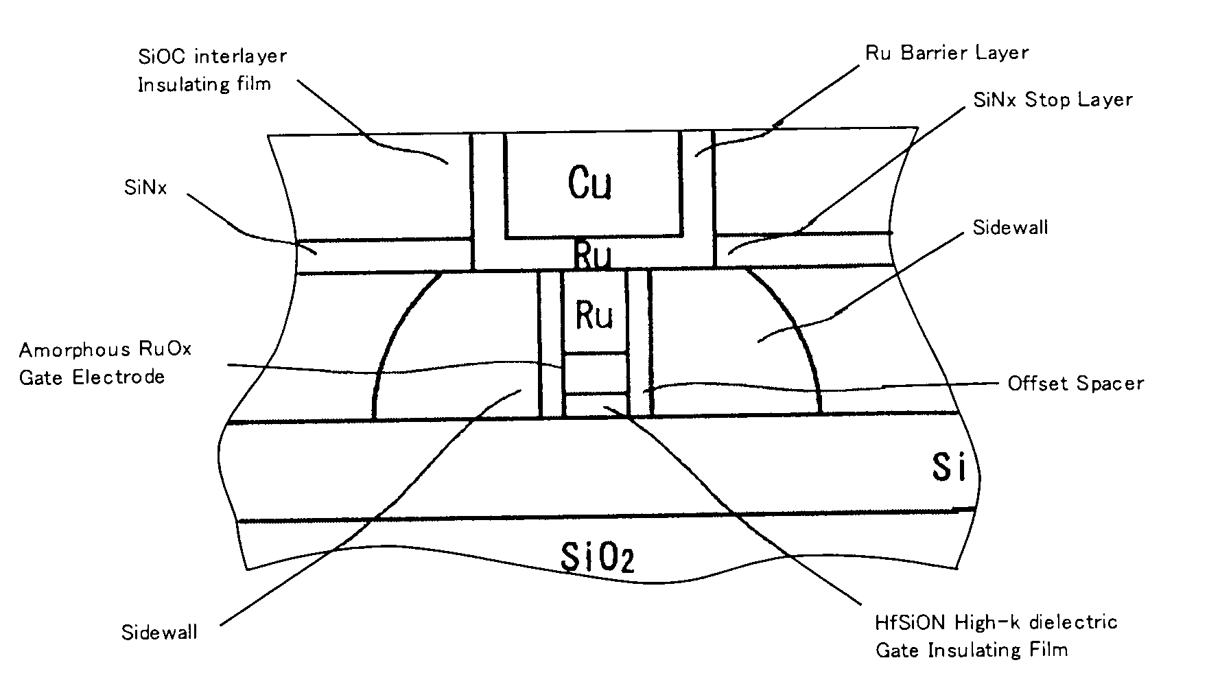
[0097]FIG. 11 shows another embodiment of the present invention and an example applying the present invention to a MISFET having a high-k gate insulating film.

[0098]The example of a MISFET shown in FIG. 11 includes Hf—Al—O—N used as a fully-depleted SOI substrate and a high-k gate dielectric film, a laminated film composed of an amorphous RuOx film and a polycrystalline Ru film used as a first gate electrode adhering the high-k gate dielectric film, and a polycrystalline Ru used as a plug connecting the first gate electrode so as to apply a voltage thereto. The MISFET has a structure in which an amorphous Ru film as a barrier metal for Cu wiring is deposited on the polycrystalline Ru film and the Cu wiring is deposited on the amorphous Ru film.

[0099]The above-mentioned embodiment describes an example using silicon, however, it is not limited to the silicon. That is, examples of semiconductors other than silicon include germanium, silicon-germanium, silicon carbide, diamond, gallium ...

embodiment 3

[0113]FIG. 13 shows another embodiment of the present invention and an example applying the present invention to a memory device having a floating gate.

[0114]The example shown in the drawing includes a Si substrate, silicon oxide, a Hf—Si—O—N film as a high-k gate insulating film, a laminated film composed of an amorphous RuOx film and a polycrystalline Ru film serving as a floating gate electrode held between the silicon oxide and the high-k gate insulating film, and an amorphous TiN film serving as a control gate electrode (a plug, barrier metal, and wiring metal are not shown in the drawing).

[0115]Note that the above-mentioned embodiment describes an example using silicon, however, it is not limited to the silicon. That is, examples of semiconductors other than silicon include germanium, silicon-germanium, silicon carbide, diamond, gallium arsenide, gallium nitride, zinc oxide, zinc sulfide, copper aluminate, chromium aluminate, titanium oxide, strontium titanate, indium tin oxid...


PUM

PropertyMeasurementUnit
Fractionaaaaaaaaaa
Fractionaaaaaaaaaa
Thicknessaaaaaaaaaa

Abstract

A desired property for a metal gate electrode layer is that it can cover a three-dimensional semiconductor structure having a microstructure with high step coverage. Another desired property for the metal gate electrode layer is that the surface of a deposited electrode layer is flat on a nanometer scale, enables a dielectric layer for electrical insulation to be coated without performing special planization after deposition of the electrode layer. Furthermore, another desired property for the metal gate electrode layer is that it has the similar etching workability to materials used in an ordinary semiconductor manufacturing process. Furthermore, another desired property for the metal gate electrode layer is that it has a structure in which diffusion of impurity is suppressed due to homogeneity thereof and the absence of grain boundaries. It was found that an amorphous metal electrode is most suitable for realizing the metal gate electrode layer satisfying the above-mentioned properties and thereby the present invention was achieved.

Description

TECHNICAL FIELD[0001]The present invention relates to a device constituting an integrated circuit and a method for manufacturing the integrated circuit, and more specifically, to a gate electrode of a transistor device.BACKGROUND ART[0002]Polysilicon is the most popular and effective material for electrodes to date and has been used to manufacture integrated circuits. This film has high reliability, and, in particular, the electric resistivity of electrodes and the position of the Fermi level thereof can be controlled by selecting a type of impurity which generates carriers and controlling a doping level. Furthermore, since the film can be deposited by CVD, the film can cover a three dimensionally structured body having a microstructure with high step coverage. Therefore, polysilicon has been the most popular and effective material to date for gate electrodes.[0003]Presently, the thickness of gate insulating films become extremely thin in accordance with a reduction of device size, ...

Claims


Application Information

Patent Timeline
IPC IPC(8): H01L29/78H01L21/28
CPCC23C16/406H01L21/28088H01L2924/0002H01L21/28273H01L23/53238H01L29/42384H01L29/4908H01L29/4966H01L29/513H01L29/517H01L29/518H01L29/66666H01L29/66825H01L29/7827H01L29/785H01L29/78642H01L29/78648H01L29/7881H01L2924/00H01L29/66545H01L29/40114
Inventor SHIMIZU, TAKASHI
Owner NAT INST OF ADVANCED IND SCI & TECH
Why Eureka
Try Eureka