[0022] Although the grain
diameter of the semiconductor fine grain is not particularly limited, it is preferable to set the mean grain
diameter of the primary particle to 1 to 200 nm, particularly preferably, 5 to 100 nm. It is also possible to mix semiconductor fine grain whose mean grain
diameter is larger than such a mean grain diameter to the semiconductor fine grain of such a mean grain diameter, scatter incident light by the semiconductor fine grain of large mean grain diameters, and improve
quantum efficiency. In this case, it is desirable that the mean grain diameter of the semiconductor fine grain to be additionally mixed is equal to 20 to 500 nm.
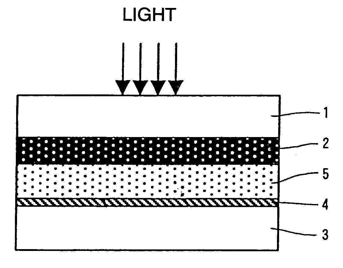
[0023] Generally, the more a thickness of semiconductor layer comprising the semiconductor fine grain increases, the more an amount of adsorbed dye per unit projection area increases, so that a capturing ratio of the light rises. However, since a
diffusion length of the injected electrons increases, a loss caused by charge recombination also increases. Therefore, although a preferable thickness of semiconductor layer exists, it is generally equal to 0.1 to 100 μm, preferably, 1 to 50 μm, particularly preferably, 3 to 30 μm. To increase a surface area of the semiconductor fine grain, remove impurities of the semiconductor layer made of the semiconductor fine grain, and raise
electron injecting efficiency upon injecting electrons from the dye into the semiconductor fine grain, for example, a
chemical process using a
titanium tetrachloride aqueous solution or an electrochemical process using a
titanium trichloride
aqueous solution can be also performed. A conductive assistant can be also added to reduce an impedance of the semiconductor layer made of the semiconductor fine grain.
[0032] A smaller
sheet resistance of the transparent conductive substrate is better. Specifically speaking, the
sheet resistance of the transparent conductive substrate is preferably set to 500 Ω / cm2 or less, more preferably, 10 Ω / cm2 or less. In the case of forming the transparent
electrode onto the transparent supporting substrate, any type of material can be fundamentally used so long as it has the
conductivity and transparency. However, it is desirable to use
indium-
tin composite oxide (ITO),
fluorine doped SnO2 (FTO), SnO2, or the like from a viewpoint that they have the
conductivity, transparency, and further,
heat resistance at high levels. ITO is preferable among them in consideration of the costs. It is also possible to combine two or more kinds of those materials and use them. To reduce the
sheet resistance of the transparent conductive substrate and improve the collecting efficiency,
metal wirings having the
high conductivity can be also patterned onto the transparent conductive substrate.
[0033] An arbitrary
electrode can be used as a counter
electrode so long as it is made of a conductive substance. An insulative substance can be also used so long as a conductive layer is formed on the side where it faces the semiconductor layer. However, it is desirable that a material which is electrochemically stable is used as an
electrode material. Specifically speaking, it is preferable to use
platinum, gold,
conductive polymer, carbon, or the like. To improve the catalyst effect of the
redox reaction, it is desirable that the electrode on the side where it faces the semiconductor layer has a
fine structure and its surface is increased. For example, in the case of
platinum, it is desirable to be in the
platinum black state and in the case of carbon, it is desirable to be in the porous state. The
platinum black state can be formed by an
anode oxidizing method, a
platinum chloride acid treatment, or the like of platinum. Carbon in the porous state can be formed by a method of
sintering carbon fine grain, a method of
sintering an
organic polymer, or the like.
[0034] The
electrolyte becomes a carrier transfer layer and is constructed by a
redox species and a
solvent. Specifically speaking, the
redox species is constructed by, for example, a combination of
iodine (I2) and an
iodine compound (
metal iodide,
organic iodide, or the like) or a combination of
bromine (Br2) and a
bromine compound (
metal bromide, organic
bromide, or the like). Further, there can be used: metal complexes such as ferrocianic
acid salt / ferricianic
acid salt,
ferrocene / ferricynium ions, or the like;
sulfur compounds such as polysodium
sulfide, alkylthiol /
alkyl disulfide, or the like;
viologen dye;
hydroquinone /
quinone; or the like. As cations of the above metal compound, it is suitable to use Li, Na, K, Mg, Ca, Cs, etc. As cations of the above
organic compound, it is suitable to use a
quaternary ammonium compound such as tetraalkyl ammoniums, pyridinums, imidazoliums, or the like. However, the cations are not limited to them and it is also possible to combine two or more kinds of those elements and use the mixture as necessary. Among them, an
electrolyte obtained by combining I2 with
quaternary ammonium compound such as LiI, NaI, imidazolium
iodide, or the like is suitable. A concentration of
electrolyte salt is preferably set to 0.05 to 5 M for the
solvent and, further preferably, 0.2 to 1 M. A concentration of I2 or Br2 is preferably set to 0.0005 to 1 M and, further preferably, 0.0001 to 0.1 M. To improve a release
voltage and a short-circuit current, various additives such as 4-tert-butyl
pyridine, 2-n-propyl
pyridine,
carboxylic acid, and the like can be also added.
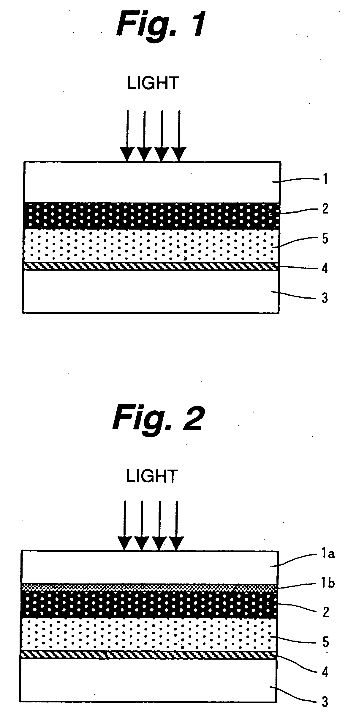
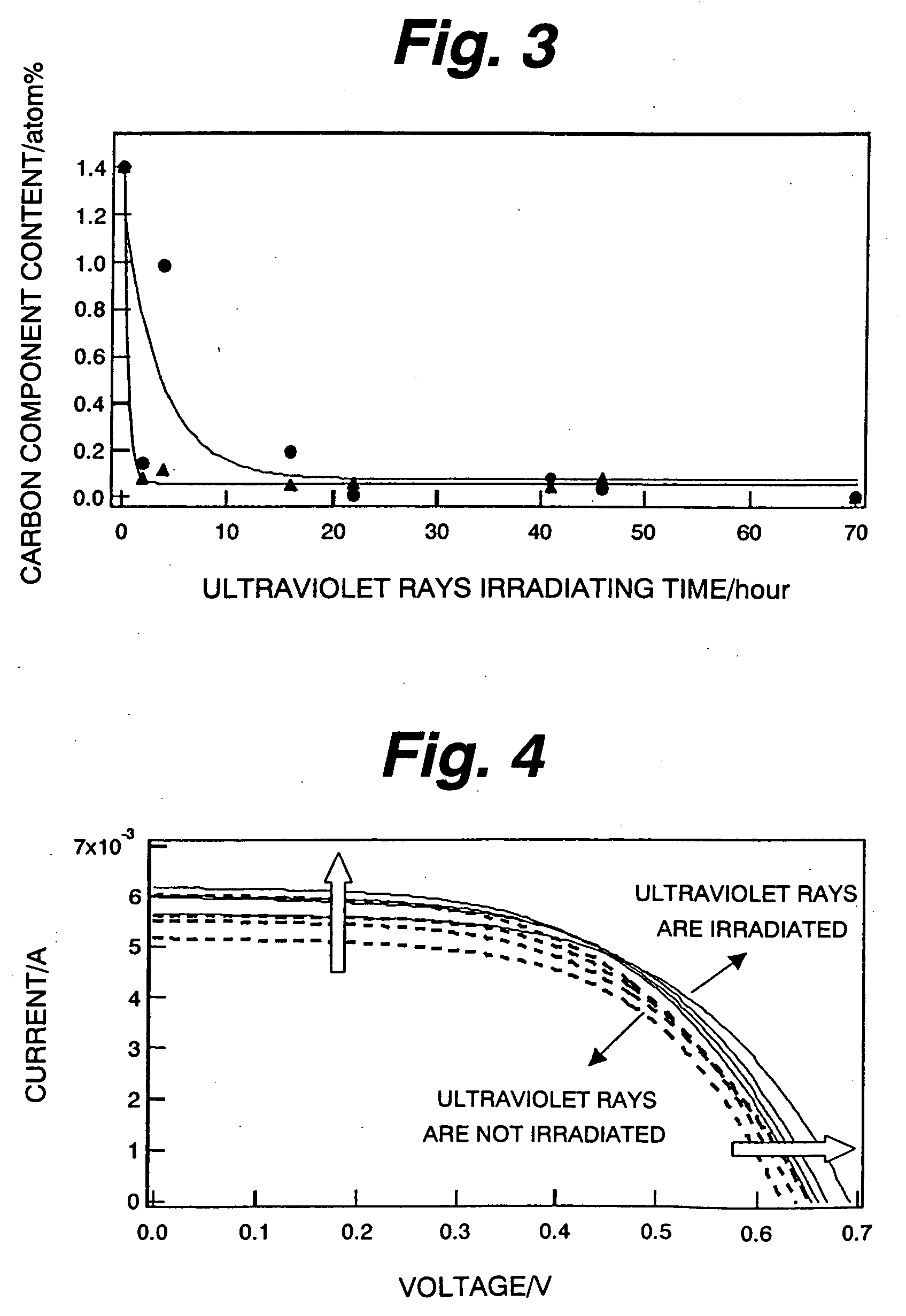
[0054] According to the invention constructed as mentioned above, the paste in which the semiconductor fine grain and the binder made of the
polymer compound are mixed is coated and sintered, thereby forming the semiconductor layer made of the semiconductor fine grain. After that, by irradiating the
ultraviolet rays to the semiconductor layer, the organic substance remaining in the semiconductor layer is oxidization dissolved by the photocatalyst effect of the semiconductor fine grain, becomes
carbon dioxide, water, and the like, and is removed. Particularly, by sufficiently irradiating the
ultraviolet rays, it is possible to realize the state where the organic substance does not substantially remain in the semiconductor layer. As disclosed in Non-
Patent Document 2, if the semiconductor fine grain is made of
titanium oxide, the surface changes to the surface having hydrophilicity (the surface hydroxyl group increases), so that a
binding force between the semiconductor fine grain increases and the
electron movement between the semiconductor fine grain becomes easy. At the same time, if the semiconductor fine grain is made of
titanium oxide, a
coupling force between the sensitizing dye and a carboxyl group is also increased due to an increase in surface hydroxyl group. The
electron movement between the dye and the semiconductor fine grain made of
titanium oxide also becomes easy. Consequently, the photoelectric conversion efficiency is improved.

