Regardless current market successes, semiconductor laser diodes, because they typically exhibit a high-degree of ‘Inhomogeneous Broadening’, have an uncertain future in several high-value market applications.
Further, inhomogeneous broadening occurs when the environment or properties of particles in an emitting sample are non-identical.
Consequently, when phonons collide with SE present with the semiconductor it undergoes a perturbation of its phase, which results in it becomes arbitrarily distributed relative to the laser field (
stimulated emission), which in turn causes the oscillating STE undergoing amplification (via
resonance) within the cavity of the
laser diode, to destabilize; thereby, causing all kinds of instabilities to manifest for the laser-emission-output.
Laser performance can also degrade with increasing ambient temperature.
Further, multimode emission results when high rates of semiconductor spontaneous-emission leads to relatively high intensities of “Amplified Spontaneous-Emission” (ASE)
modes occurring below the
lasing threshold of the
laser diode.
Moreover, for the VCSEL diode, an inhomogeneously broadened
gain results instead, in an unstable state of polarity for it's laser-emission-output.
This makes it practically impossible for the VCSEL diode to be used in polarity sensitive applications like
magneto-optic high-density data storage.
Since most types of lasers may be unambiguously classified as being either homogeneously or inhomogeneously broadened, the dual character exhibited by the semiconductor
laser diode makes its particular
physics interesting and somewhat complicated.
Further, because of gain-clamping, intensity fluctuations have negligible direct effect on the line-width; however, they do cause fluctuations in the carrier-density.
Since the
refractive index change due to carrier-density at the gain-peak is large in a semiconductor gain-medium, the density fluctuations cause substantial index fluctuations, which, in turn, lead to fluctuations in phase.
Of course, doing so may be impractical because the needed optical elements are likely to be considerably larger than the laser diode.
In the lateral (ŷ) direction, the optical-field confinement is often weaker, leading to substantial
astigmatism in the laser-emission-output.
This, as a direct consequence of gain-saturation, leads to the formation of concentric variations in the
refractive index distribution, which, in turn, results in the self-focusing of the laser field.
Typically,
filamentation makes a
noise contribution that keeps laser diodes suffering from it from being utilized in current application.
However, for a laser diode that has a large area gain-volume, the self-focusing effect causing
filamentation, being comprised as having a very high-intensity
optical field, would most likely introduce what is commonly called “Catastrophic Optical Damage” (COD) to the laser diode's molecular structure, causing it to fail entirely.
Filamentation is just one
instability made to occur when spontaneous-emission makes its phase perturbating contribution to resonant laser fields.
These
resonator designs, some of which are described below in much detail, failed because they were designed to treat one, maybe two, particular instabilities rather than the cause of the destabilization.
However, because these approaches fail to neutralize the arbitrary phase
instability contributed to
resonance by the
acoustic phonons and the spontaneous-emission that occur within all semiconductor laser diodes, they fail to stabilize the amplified
resonance of intracavity stimulated-emission, which is seriously degrading the performance of current laser diodes.
Unfortunately, even after being redesigned to provide for a laser-emission-output that exhibits a stable polarity, the VCSEL still suffers from the same polarity switching
instability problem it did before being redesigned.
This prevents their use in applications, which require high-power laser-emission output into a single transverse spatial cavity mode at a single frequency.
Furthermore, EELs exhibit a significant degree of
astigmatism, and a beam
aspect ratio that is generally large making it difficult to focus the beam to a small spot size preventing EELs from being used in those applications that require a focused beam output.
Further, poor beam quality in EELs also makes frequency doubling of the laser-emission-output, using
nonlinear optical materials, difficult and inefficient.
Further, EELs, because of their much longer cavity lengths and significantly larger gain-volumes, can only be internally modulated at around 2.3-Gbits / ps before they begin to suffer significantly from dispersive
pulse broadening effects, which has prevented them from being used in applications requiring a high-degree of internal modulation for the laser-emission-output transmission of data signals.
Widely adapted for LANs are the selectively oxidized VCSEL diodes, which use an
oxide aperture located within its vertical cavity to produce strong electrical and optical confinement, enabling high electrical-to-optical conversion efficiency, however, a
design strategy that only provides minimal
modal discrimination—allowing emission into multiple transverse spatial
modes.
However, because selectively oxidized based VCSEL diode designs exhibit a high-degree of index confinement, stable single low-order transverse spatial mode operation in selectively oxidized VCSELs is a challenging task at best.
A
disadvantage, however, is that the etched relief requires careful alignment to the
oxide aperture or it could greatly result in an increase of optical
scattering loss for the fundamental transverse cavity
modes, as manifested by the relatively low (i.e., less than 4-mW) single-mode laser-emission output powers that have been reported.
Creating this structure, however, requires a detailed understanding of the
oxidation process, and produces additional loss for the much-desired fundamental trans-verse cavity mode.
However, the problem here is that using even longer cavity spacers can also introduce multiple longitudinal cavity modes (i.e., generally called spatial hole burning) negating the VCSEL's greatest contribution to semiconductor laser diode application, but has resulted in single transverse cavity mode operation up to nearly 7-mW.
However, this is all rather academic, because in order to achieve stability for a laser-emission-output into a single fundamental transverse cavity mode of low-order (i.e., preferably TEM00), the required amounts of loss needed in order to discriminate the desired mode ultimately introduce so much loss that the laser-emission-output levels never exceed a few milliwatts of power for typical gain-regions 13-μm in
diameter, more or less making these devices incapable of any real world application.
Further, the 13-μm
diameter size used for the VCSEL's gain-region typically cannot be exceeded in an attempt to increase gain because it would introduce the onset of higher-order transverse spatial cavity modes below threshold regardless of any particular loss mechanism utilized to eliminate them.
Interestingly, both the
modal loss and
modal gain design approaches, though they have had some moderate success, do not completely resolve the multi-mode operational issue for the VCSEL because they only treat the symptoms of the instability not the cause.
This approach also requires greater fabrication complexity, however, it is anticipated that higher performance can be reached with further refinement of process parameters.
Further, in order to achieve a stability for a laser-emission-output into a single fundamental transverse cavity-mode of low-order (i.e., preferably TEM00), the required amounts of loss needed in order to discriminate the desired cavity mode ultimately introduces so much loss that the laser-emission-output levels never exceed only a few milliwatts of output power for a gain-region 13-μm in
diameter, making these devices incapable of any real world application.
Moreover, prior art further teaches that these techniques have resulted in laser-emission-output levels being limited to less than 5-mW.
Apparently, a major drawback with existing VCSEL design is the performance of their laser-emission-output levels for single mode devices, which are typically very small.
This is why the current market does not see any commercially available
Indium-
Phosphide based long-
wavelength 1.550-μm VCSEL diodes.
Further, it is quit clear that the VCSEL diode suffers from several major performance issues yet to be resolved, which limits its application to non-proprietary low-power, multimode, and visible
wavelength operation.
However, operation of any VCSEL diode having such a large gain-region diameter generally carries with it the penalty of a laser-emission output beam exhibiting higher-order transverse cavity modes and related multiple frequencies, and for devices having gain-region diameter sizes that exceed 1
millimeter in size suffer from the
filamentation problem that ultimately leads to COD.
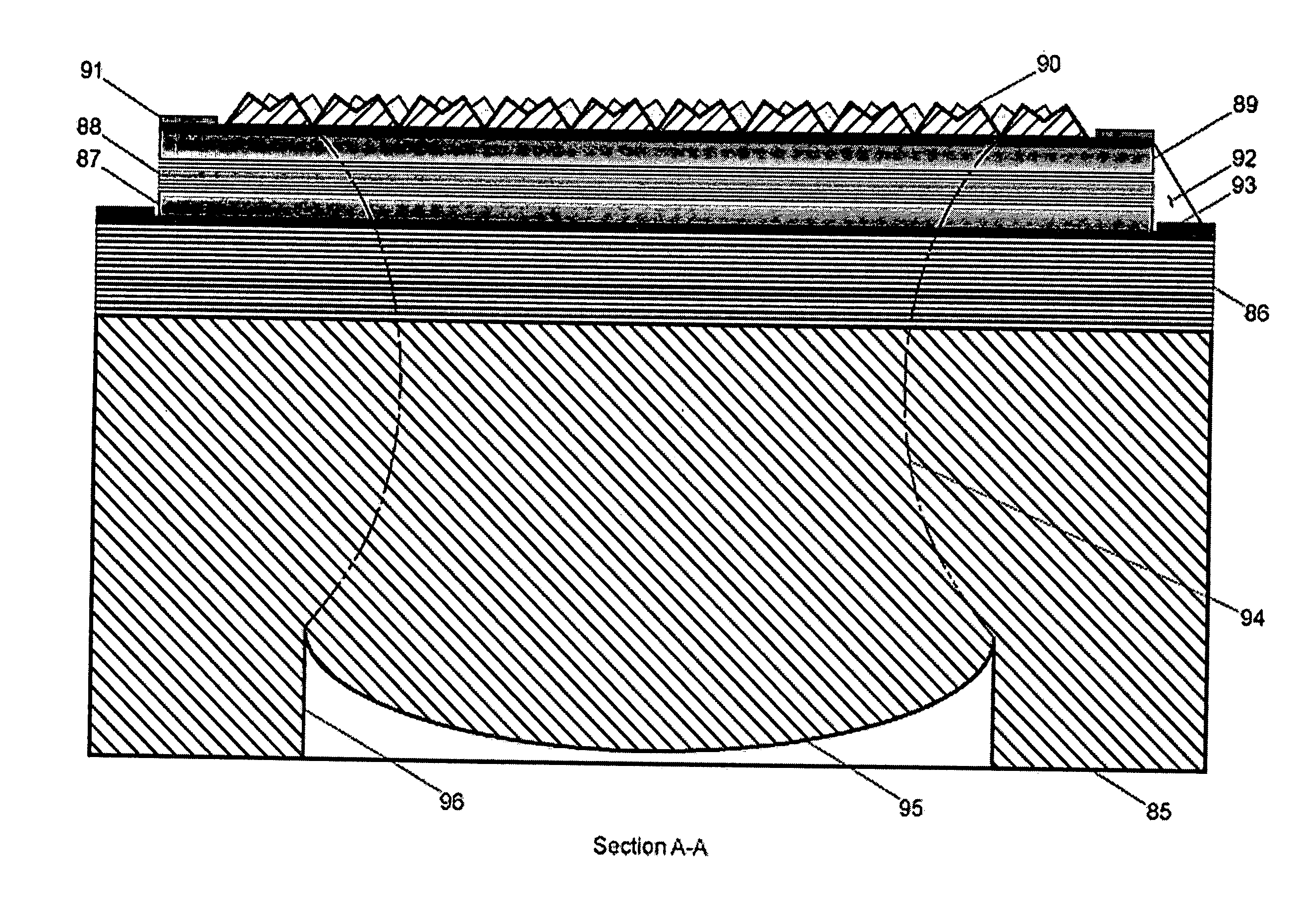
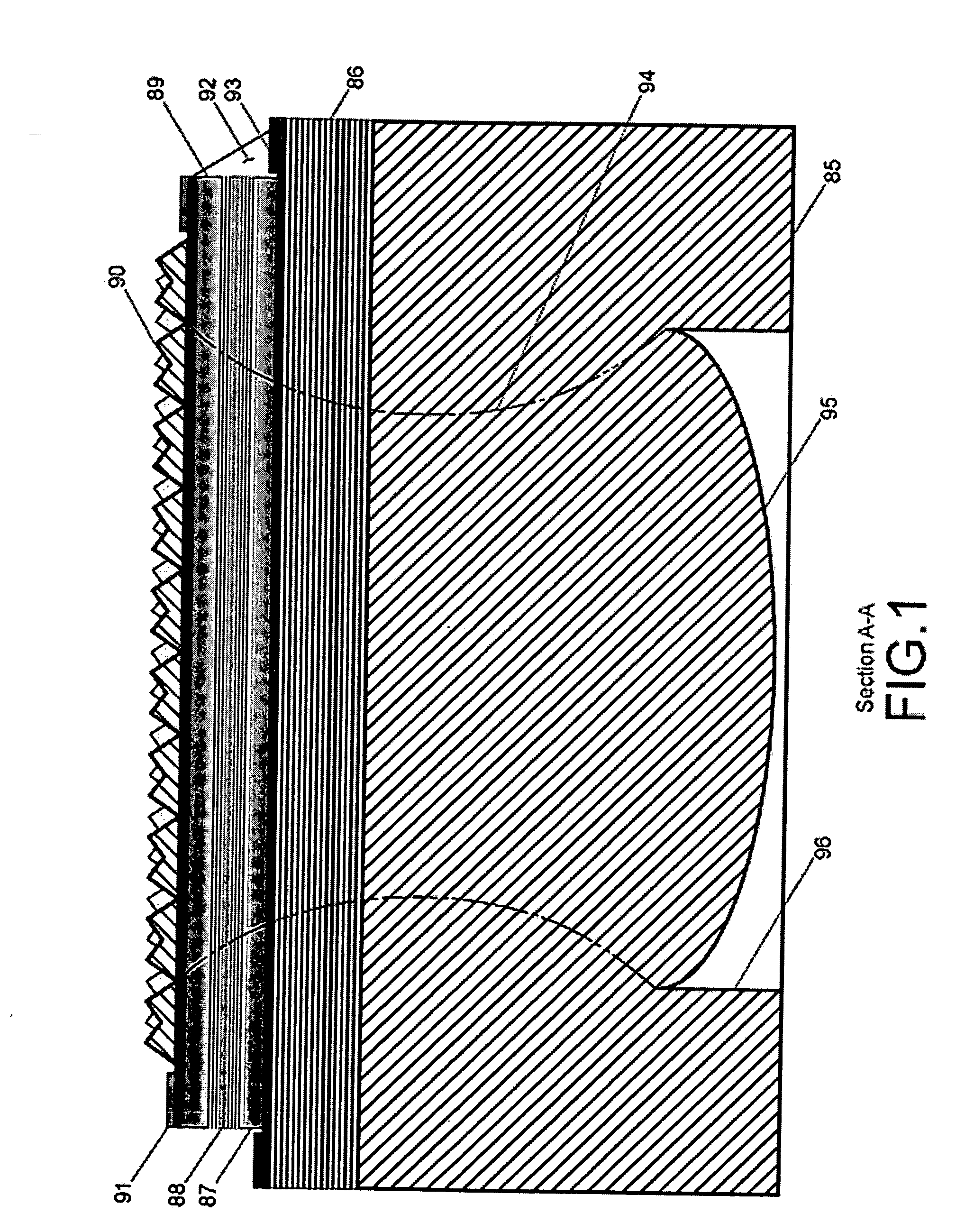
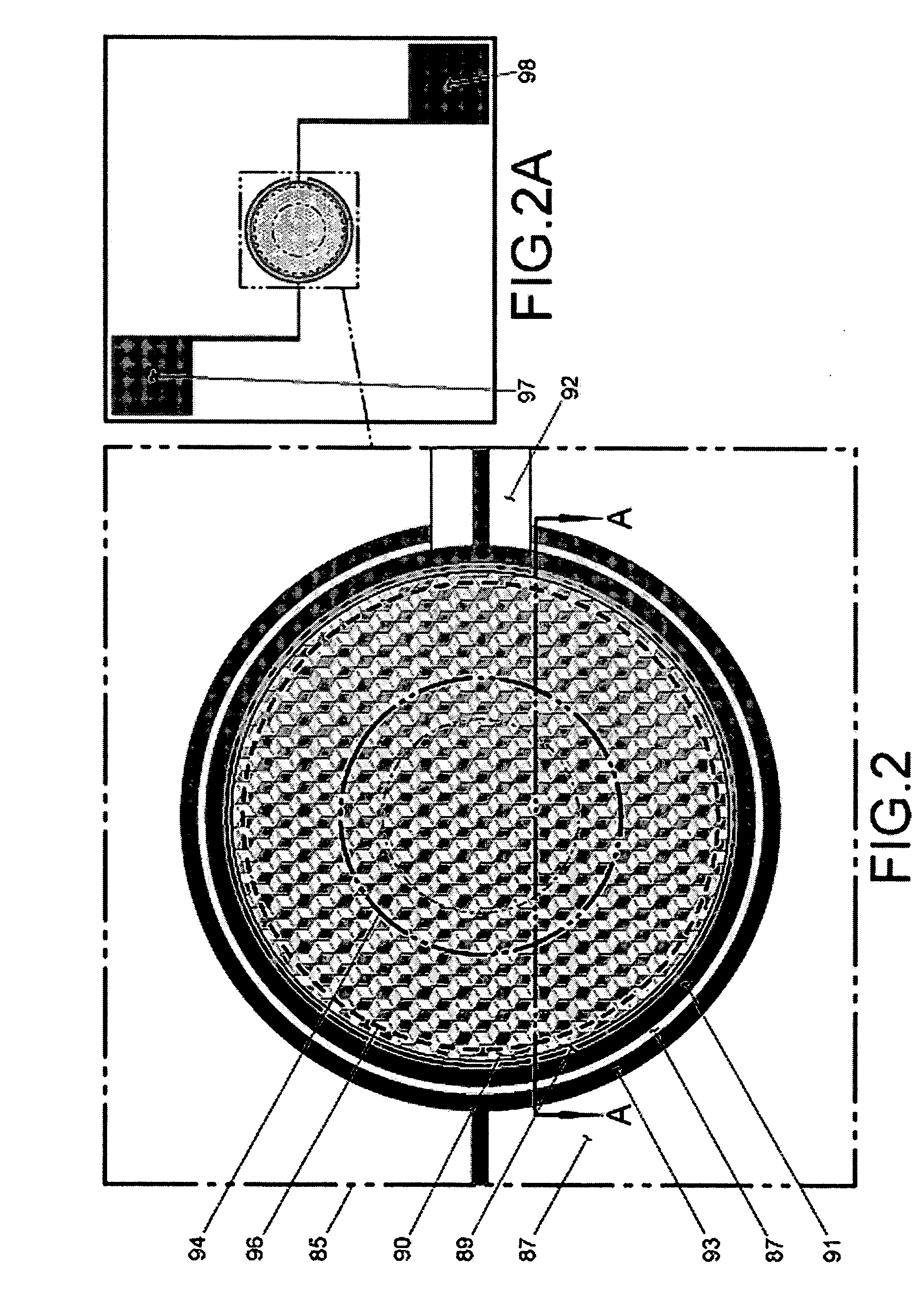
Previous work on
external cavity vertically emitting semiconductor lasers typically resulted in low output power.
Furthermore, while the NECSEL design approach is capable of producing high-power laser-emission-output into a single fundamental transverse cavity mode it suffers from two major flaws that limit its use to non-telecom and non-Datacom application (i.e., for use in
optical fiber signal regenerative pumping).
Because the NECSEL uses DBR multi-layered mirror structures to provide for optical feedback the device is limited to only near infra-red and visible
wavelength application.
Because the NECSEL resonator is configured to utilize internal
thermal lensing (i.e., resulting from carrier induced change of
refractive index and the gain-saturation that occurs for large semiconductor gain-volume) to provide for a stable resonance capable of lasing into a single fundamental transverse cavity mode at higher laser-emission output power, it cannot provide for internal modulation speeds of around 2.3-Gigabits / ps—soon to exceed the 10-Gigabits / ps that are typically being required for present and near-future low-cost
fiber-optic application (e.g., such as Passive Optical Networks,
Fiber-To-The-Home, and
Fiber-To-The-Premises).
Moreover, to define this problem further, let us take a quick look at
ion-implanted VCSELs; they typically suffer from internal modulation delays as large as 1-μsec or more; moreover, the laser turn-on
delay for these devices is caused by intracavity thermal lens formation.
In addition, prior art also teaches many examples of narrow-stripe EEL diodes, which emit high-quality
laser beams, but have several drawbacks that limit their use in high-value applications.
The main reason for this is lateral mode instabilities, which arise because high output power and single mode operation have contradictory design requirements.
Furthermore, typical heterostructure only support the lowest transverse cavity modes.
We consider multilateral mode operation to be instability because it gives rise to spectral broadening and high spatial frequencies in the
lateral field distribution.
The detrimental effects of filamentation are material damage due to increased peak-intensity, and increased loses via
spontaneous emission due to a reduced overlap between lasing
optical field and the gain-region.
These semiconductor laser diode devices, however, are quit sensitive to temperature distribution, which in turn causes their spatial oscillation modes to become unstable (i.e., the instability sometimes called spatial mode hoping by those well versed in the art).
Moreover, what should be apparent by now to the reader is how difficult it is to achieve both a single low-order fundamental transverse cavity mode oscillation and a high-power laser-emission-output for conventional semiconductor laser diode devices.
For example, prior art teaches that the semiconductor laser diode device describe above has a design configuration that finds it difficult to emit
laser light with higher output power into a single transverse cavity mode.
Moreover, the pillar lasers of Jewell et al. suffer from several problems, e.g.
electrical contacts need to be formed onto the top of the high aspect-ratio pillars, which posses a fabrication problem.
Additionally, for small pillar laser diodes, the relatively large sidewalls cause excessive recombination.
Consequently, heat cannot be efficiently dissipated from the pillar laser structures, causing degradation in laser-emission-output performance.
Work is progressing on this approach and on regrowth using insulating AlGaAs, which would help solve the recombination and
thermal dissipation problems, but currently the results are not very satisfactory.
However, using the above-mentioned approach Orenstein et al. might have retained the current gain-guiding of Jewell et al., but as a result sacrificed any index guiding advantages, since the protons did not have a significant effect on the refractive index of the
implant area.
Recent experiments, however, has demonstrated that this technique does not work.
Aside from efficiency and thermal problems, the sparsely connected filaments are not likely to be phase-locked or even to have the same frequency.
Therefore, a large area surface-emitting laser tends to lose its laser characteristics.
However, such a structure and associated
processing produce very
high surface recombination on the sides of the pillars because of the large surface-to-volume ratio.
Resulting in a high degree of
signal noise, which has keep these semiconductor laser diodes from being used in high-value applications; e.g., applications such as
Telecommunications, Datacom, and the convergent “Passive Optical Networks” (
PONs).
However, this approach employs an edge-emitting laser structure and has a large
beam divergence angle (i.e., sometimes referred to as the
diffraction angle) along the direction that is perpendicular to the laser surface, as well as a much higher
optical power density at the laser
facet that it is susceptible to catastrophic mirror damage.
This can require correction and collimating, which can be expensive or otherwise impracticable or undesirable.
In addition, prior art also teaches that due to the nature of the curved
grating, the laser-emission-output beam has a spatial phase-difference distribution, which reduces
optical beam quality.
Unfortunately, few convenient laser sources operate in the mid-IR spectral region.
As noted above, for example, bipolar semiconductor laser diodes, including
quantum-well laser diodes, have too large a bandgap, making it difficult, if not impossible, to obtain laser operation at mid-IR wavelengths.
Some semiconductor laser diodes can operate in this
wavelength range, but they require special cooling to a very low-temperature, which can be costly.
It is difficult, however, to achieve a spatially coherent, single-mode, high-power laser-emission-output using conventional edge-emitting QC laser structures as the source of mid-IR
radiation.
A high injection
current density will cause severe device heating, thus significantly limit the maximum laser-emission-output power, and therein, reduce the laser's lifetime.
Moreover, prior art further teaches that for any BALD device, regardless what type of semiconductor gain-region it might use, it is very difficult to maintain single mode operation under high-current injection operation because of the carrier induced refractive index change that causes the filamentation problem, which, as previously stated, hastens the onset of multi-moded lasing.
Moreover, the self-induced filamentation effect produces a multi-spatial cavity mode laser-emission-output, which diminishes the laser's power and performance.
The multi-mode laser emission is very difficult to focus, which is especially problematic when a long propagation distance or a very small focus
beam size is required.
Consequently, the multi-mode laser emission is less coherent and therefore, very difficult to use in several high-value applications such as
Telecommunications.
Unfortunately, increasing the width of the gain-region typically leads to spatially incoherent operation at
high current injection levels.
In conclusion, while prior art shows conclusively that QC semiconductor lasers can made somewhat stable, they still suffer from the same
phase perturbation problem contributed by
spontaneous emission that all other semiconductor lasers suffer from regardless any improvement.
In addition, prior art also teaches that the different transverse spatial cavity modes of an optical resonator will typically have different resonant
optical frequencies, which is characteristically detrimental for both active and passive cavity applications requiring
spectral purity.
Problems begin to arise, however, when we try to design high-powered laser-emission-output capable VCSELs; wherein, a contradictory contention arises between the desire to increase modal volume and
beam diameter size, and the desire to suppress oscillation of the higher-order transverse cavity modes.
Further, prior art teaches that for passive cavity devices, the transverse spatial mode problem is more intractable, since the high-degree of freedom associated with the design of the gain-medium is not present.
The inclusion of
optical fiber, however, tends to complicate device integration, creates
fiber-
coupling requirements, and does not resolve all of the spatial cavity mode problems present.
These spatial filters, however, can also introduce loss for the fundamental transverse spatial modes as well, and therefore require precise alignment.
Therefore, as prior art suggests, a
confocal MOEMS micro-cavity configuration would require mirrors with correspondingly small radii of curvature (i.e., tens of micrometers), which are difficult to fabricate and have small cavity mode sizes, which are also difficult to align.
In conclusion, prior art clearly shows that the SEL based semiconductor laser diodes as described above, as described in the included materials, and mentions, while in some cases might provide for low-order fundamental transverse spatial cavity mode laser-emission-output, they all typically suffer from three major performance issues:
Because they do not neutralize the phase perturbations contributed by
spontaneous emission to resonance, the laser-emission-output remains unstable manifesting multiple instabilities (e.g., spatial
mode hopping, spectral
mode hopping, polarity switching, high threshold currents, filamentation, multi-transverse operation at threshold, multi-longitudinal operation at threshold, spatial hole burning, spectral hole burning, low-power laser-emission-output, overall degradation of laser diode performance, and single low-order fundamental transverse spatial cavity mode being virtually un-attainable over a wide range of power levels;
Because the solutions described above and in the included references focus on introducing loss for high-order transverse spatial cavity modes, the overall
power performance of the laser diode is seriously degraded to the point where these laser diodes only produce around 2-mW to 3-mW of laser-emission-output power and therefore, not applicable for most current high-valued application; e.g., applications such as optical Telecommunication and
Data transmission; and
Because these devices (mostly EELs) suffer from intra-cavity pulse-broadened dispersion (i.e.,
chirp) they have reached their internal limits for data modulation and therefore, can not transmit data any faster than just a few Gigabits / ps.
Consequently, this limits them to low-valued applications; e.g., such as multimode
fiber optic LANs, fiber channel interconnects, and other non-proprietary Datacom and Enterprise based application.

