
Bandgap-shifted semiconductor surface and method for making same, and apparatus for using same

a technology of semiconductor surface and band-gap-shifted semiconductor, which is applied in the direction of photovoltaic supports, electrolysis components, electrolysis processes, etc., can solve the problems of carbon-based energy pollution, high cost, and high cost of carbon-based energy, and achieves high efficiency, better matched, and high stress in titania

Active Publication Date: 2008-12-04
NANOPTEK CORP
View PDF25 Cites 10 Cited by
  • Summary
  • Abstract
  • Description
  • Claims
  • Application Information

AI Technical Summary

Benefits of technology

[0183]FIG. 19 illustrates schematically one method for large scale manufacture of photoactive electrodes of the present invention comprising titania films on undulating substrates. In FIG. 19, a polycarbonate substrate or a titanium foil (also known as a coil in the industry) 1951 is delivered from a roll (indicated at 1950) into an embossing machine, in which a stamper 1954 containing the desired undulation shape and pattern 1954′ and wrapped around roller 1953, is embossed into the polycarbonate or the titanium coil using known embossing techniques that may include heat and / or solvents to varying degrees. The stamper is typically a nickel replica grown from a master, and may be coated with a harder material such as diamond-like carbon coating when working with titanium coil. The master is typically a photoresist or photoablative polymer on a glass or silicon substrate, into which the desired undulations have been formed by one of the following methods: contact lithography, projection lithography, interferometric lithography, or laser beam recording. Finally, the embossed polycarbonate web is coated in a vacuum chamber 1955 with e-beam 1956 (the preferred method, although others can of course be used) sputtering, ion-assisted deposition, or thermal evaporation, from a target 1957. Material 1958 from the target then deposits onto the web 1951. The result is that the polycarbonate or titanium emerges from the chamber coated with, in this example, titania 1959. In FIG. 19, sealing means 1960 and 1961 are provided to maintain a vacuum lock on the web, but the entire roll can alternatively be in the coater at one time. Sol gel or chemical vapor deposition are also possible means of coating. Also, instead of roll manufacture, the polycarbonate substrates can be injection / compression molded to the stamper. All of these techniques are known in the optical data storage and other industries. It is an important advantage of the present invention that bandgap-shifted titania can be manufactured with existing infrastructure in low-cost mass production methods, because any solar energy conversion application requires large area, low cost devices. However, in the case where the base material is titanium foil, it will be seen that it is advantageous to use a titania forming method other than vacuum coating.
[0184]The second main method for the formation of photoactive electrodes of the present invention will now be discussed, this second method, as already mentioned, comprising etching of titanium metal to form nano-structures in the titanium, followed by anodizing or oxidation, or both, to convert the etched titanium to titania, preferably in the anatase form. As a preliminary matter, some theoretical discussion of the variation of titania bandgap with physical parameters will be given; this theoretical discussion is of course also applicable to nano-structured titania coatings produced by the first method of the present invention.
[0185]As already mentioned, it is well known that the bandgap of a semiconductor changes with change in volume of its lattice, this change of volume being caused by, inter alia, temperature change or applied pressure. To understand how this general principle applied to the anatase form of titania, changes in the bandgap of this material were modeled as a function of biaxial strain. To achieve quantitatively accurate results, the GW approximation was used to calculate the bandgap. The GW approximation (GWA) is an approximation made in order to calculate the self-energy of a many-body system. The approximation is that the expansion of the self-energy Σ in terms of the single particle Green function G and the screened interaction W can be truncated after the first term. We used ABINIT software to achieve the GW approximation (ABINIT is a free software package for physicists, distributed under the GNU General Public License, whose main program allows the total energy, charge density, and electronic structure of systems made of electrons and nuclei (molecules and periodic / crystalline solids) to be calculated within Density Functional Theory (DFT), using pseudopotentials, and a plane wave basis.)
[0186]It was also important to determine the effective mass of the charge carriers in the semiconductor, since large effective mass charge carriers can lead to higher recombination of photogenerated electron-hole pairs and hence to reduce efficiency of the electrode. Accordingly, density functional theory modeling was used to produce complete band structure plots which could be used to estimate the effective mass of the charge carriers. Theoretically, the bands follow a quadratic relationship around the conduction band minimum and valance band maximum energies. The curvature of this quadratic is inversely proportional to the effective mass. Integrating ASTM International (originally known as American Society for Testing and Materials) solar irradiance data and assuming 100% photon conversion efficiency leads to the maximum achievable solar-to-hydrogen conversion efficiency. Using the GW modeling result from above further allows us to model this maximum efficiency as a function of total pressure. The band gap of anatase at zero pressure was assumed to be 3.2 eV, corresponding to a maximum efficiency of about 3.7%.
[0187]FIG. 14 shows the change in bandgap ΔEGap with pressure derived from the GW approximation. The calculation indicates that the bandgap is expected to change linearly as a function of the applied pressure at a rate of 0.0686 eV / GPa. Thus, a pressure of about −10 GPa (a negative pressure denoting a material in tension) reduces the bandgap of anatase from 3.2 to about 2.5 eV. FIG. 15 shows the expected increase in photolytic efficiency resulting from the bandgap reductions with pressure shown in FIG. 14; it will be seen from FIG. 15 that negative pressure of about −10 GPa is expected to increase the efficiency of the electrode about five-fold, from about 3.7 percent to about 20 percent.
[0188]From the anatase structure, there can be derived the full band structure plot shown in FIG. 16A. FIG. 16B shows an enlarged view of the part of FIG. 16A indicated by the arrow, and shows only the top of the valance band and the bottom of the conduction band. FIG. 16B also shows the quadratic fits used to calculate the effective mass of the holes and electron charge carriers, denoted mh and me respectively.

Problems solved by technology

The ills of our carbon-based energy are well-known: pollution of land and oceans, air pollution, and the global warming that is likely caused by the latter.
In addition, there is the growing dependence on foreign oil (presently at 46%, up from 27% during the Oil Embargo during the Carter administration) with the economic, political, and human costs that result from that dependence.
However, the losses of the solar cell in converting sunlight to electricity, combined with the losses in the electrolytic splitting of water into hydrogen and oxygen, make for low efficiency overall.
Further, the cost of the apparatus and lifetime of the components make the economic viability dim at this time.
However, the threshold energy for this reaction is 6.5 eV, so direct photodissociation is not possible.
Even so, their energy conversion efficiencies were low.
This again reduces economic viability.
In their model, the low quantum efficiency of titania is not due to inefficient carrier transfer, as others had shown that this was close to 100% with platinized −Pt cathodes and illuminated titania anodes, but rather to insufficient band-bending at the titania surface to cause efficient separation of the electron-hole pairs.
Such a process requires solvents and temperatures incompatible with polymer substrates.
This electrolyte is non-aqueous and somewhat volatile, so packaging, cell lifetime, and effect on the environment remain problematic.
Most importantly, such a device provides no direct access to the titania photocatalytic surface, and so cannot be used for hydrogen production, detoxification, or disinfection.

Method used


Image

  • Bandgap-shifted semiconductor surface and method for making same, and apparatus for using same
  • Bandgap-shifted semiconductor surface and method for making same, and apparatus for using same
  • Bandgap-shifted semiconductor surface and method for making same, and apparatus for using same

Examples


example 1

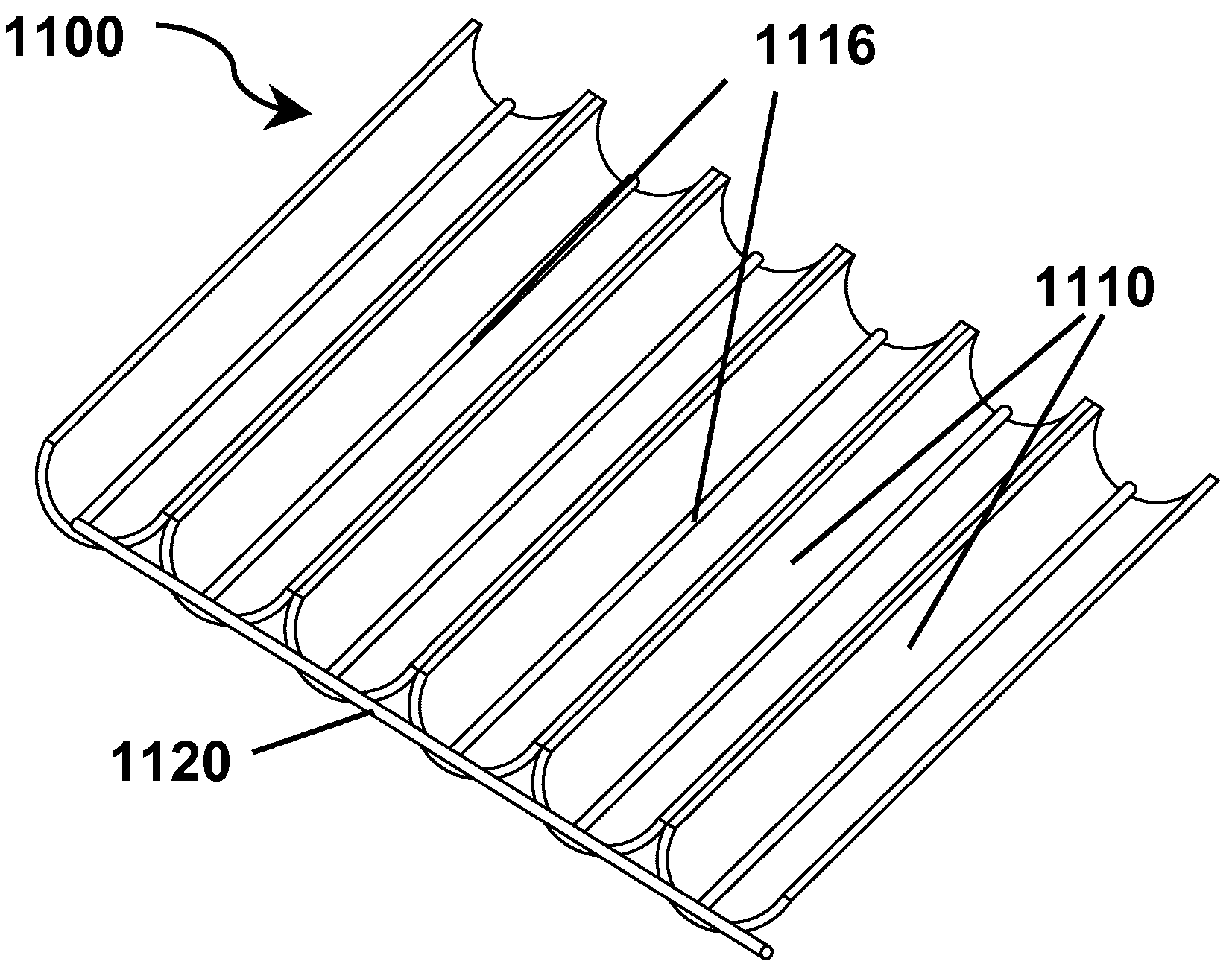
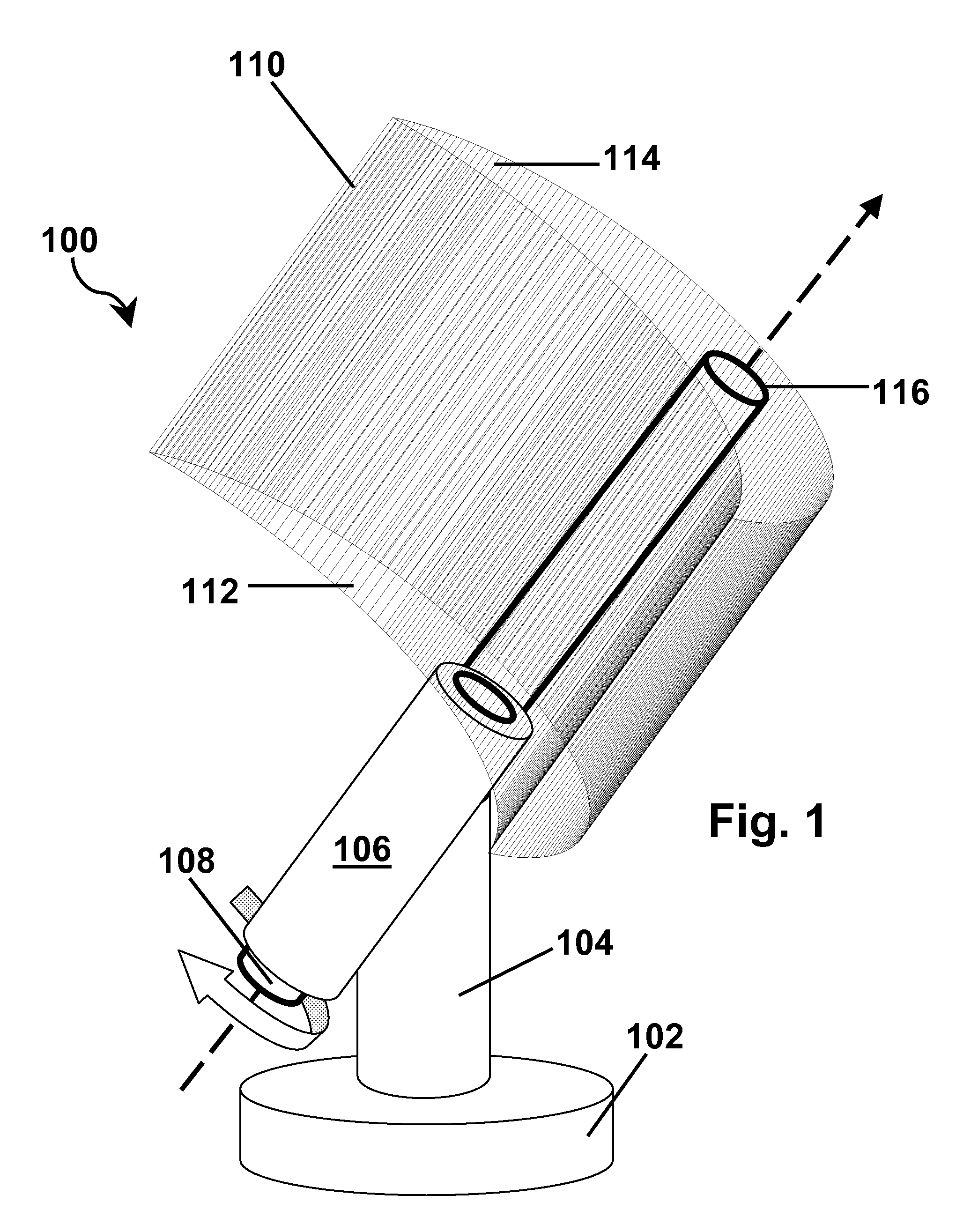
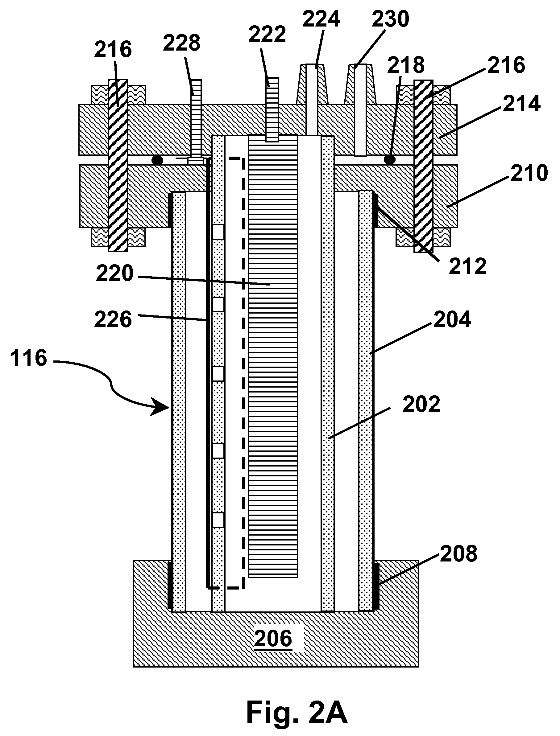
[0240]This Example illustrates the effects of illumination conditions, bias voltage and temperature on the efficiency of hydrogen production and conversion efficiency of an apparatus as shown in FIGS. 1-2 and 7.

[0241]An apparatus as described above with reference to FIGS. 1-2 and 7 was subjected to artificial solar illumination conditions of AM 1.5 and AM 0.0, where AM means Air or Atmospheric Mass, the amount of atmosphere through which the sunlight must travel to reach the ground. So, AM 1.5 is typical for sea level conditions, while AM 0.0 is for a “space” application such as orbiting satellites. with the core assembly 116 maintained at either 25 or 80° C. and with varying bias voltages applied between the photoactive anode 226 and the cathode 220. In these tests, the bias voltage was not supplied by the photovoltaic strip 602 (FIG. 7) in order to permit the illumination of the photovoltaic strip and the bias voltage to be controlled independently. FIG. 32A shows the rate of hydr...

example 2

[0243]This Example illustrates (see FIG. 33) the effects of bias voltage on conversion efficiency of an apparatus as shown in FIGS. 1, 2 and 7, as a function of the electrolyte composition. The best results, i.e. highest hydrogen production efficiency, are obtained with either an acidic electrolyte or a salt water electrolyte. The basic potassium hydroxide electrolyte performs best at zero voltage bias, but underperforms at higher voltage bias.

[0244]The photoactive titania electrodes of the present invention can be used in any application in which photoactive titania electrodes have hitherto been used, as discussed in detail in the aforementioned parent application.

[0245]In summary, this invention provides for shifting the optical bandgap of a semiconductor into longer optical wavelengths by stressing the semiconductor, where the semiconductor is a thin film, and where the stress is strain caused by some or all of the following: conditions under which the thin film is formed, the sh...


PUM

PropertyMeasurementUnit
thickaaaaaaaaaa
temperatureaaaaaaaaaa

Abstract

Titania is a semiconductor and photocatalyst that is also chemically inert. With its bandgap of 3.2 and greater, to activate the photocatalytic property of titania requires light of about 390 nm wavelength, which is in the ultra-violet, where sunlight is very low in intensity. A method and devices are disclosed wherein stress is induced and managed in a thin film of titania in order to shift and lower the bandgap energy into the longer wavelengths that are more abundant in sunlight. Applications of this stress-induced bandgap-shifted titania photocatalytic surface include photoelectrolysis for production of hydrogen gas from water, photovoltaics for production of electricity, and photocatalysis for detoxification and disinfection.

Description

REFERENCE TO RELATED APPLICATIONS[0001]This application is a continuation-in-part of copending application Ser. No. 10 / 424,259, filed Apr. 26, 2003 (Publication No. 2003 / 0228727), which claims benefit of Provisional Application Ser. No. 60 / 380,169, filed May 7, 2002. The entire disclosures of both these applications are herein incorporated by reference.BACKGROUND OF INVENTION[0002]This invention relates to a bandgap-shifted semiconductor surface, and a method for making same. This invention also relates to photocatalytic surfaces used in the process of photoelectrolysis, photovoltaics, and photocatalysis, and more specifically to induction and management of stress in a thin titania film photocatalytic surface to match the band gap of the titania more efficiently with the solar spectrum at the earth's surface for photoelectrolysis, photovoltaics, and photocatalysis.[0003]For general background information relating to this invention see:[0004]1. www.colorado.edu / ˜bart / book / solar.htm: ...

Claims


Application Information

Patent Timeline
Patent Type & Authority Applications(United States)
IPC IPC(8): H01L31/0224
CPCC25B1/003C25B15/02H01L31/06H01L31/0547Y02E60/368H02S20/00H01L31/0543Y02E10/52C25B1/55H02S20/32Y02E60/36
Inventor GUERRA, JOHN M.THULIN, LUKAS M.
Owner NANOPTEK CORP
Learn More