[0025] The following embodiments are described in sufficient detail to enable those skilled in the art to make and use the invention. It is to be understood that other embodiments would be evident based on the present disclosure, and that
system, process, or mechanical changes may be made without departing from the scope of the present invention.
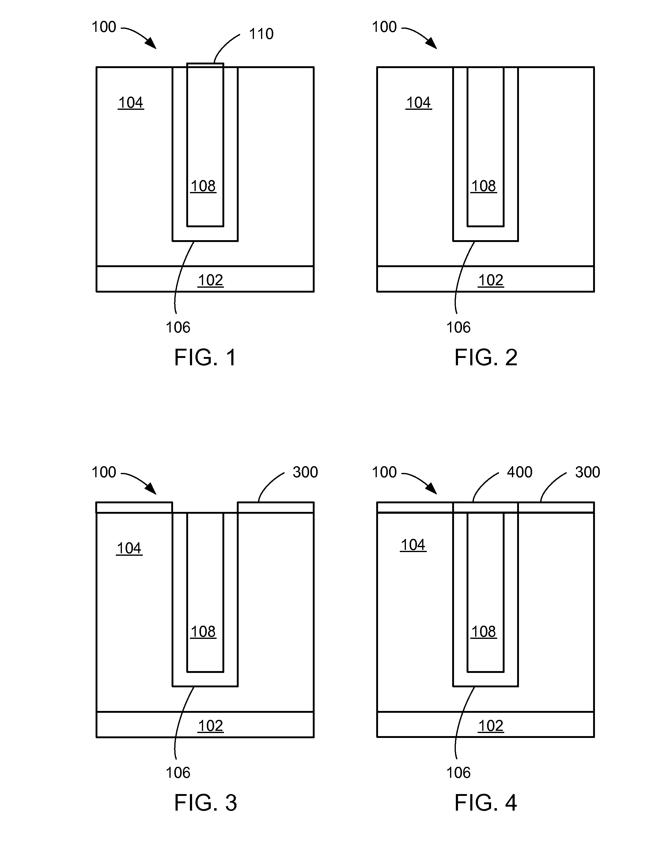
[0015]FIG. 1 is a
close up view of a semiconductor interconnect after a CMP step according to a first embodiment of the present invention;
[0016]FIG. 2 is a
close up view of the semiconductor interconnect after an
oxide removal step according to a first embodiment of the present invention;
[0017]FIG. 3 is a
close up view of the semiconductor interconnect after a hydrophobic layer formation step according to a first embodiment of the present invention;
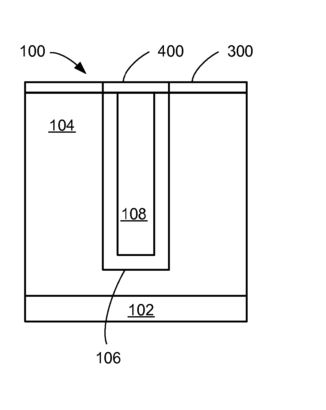
[0018]FIG. 4 is a close up view of the semiconductor interconnect after a capping step according to a first embodiment of the present invention;
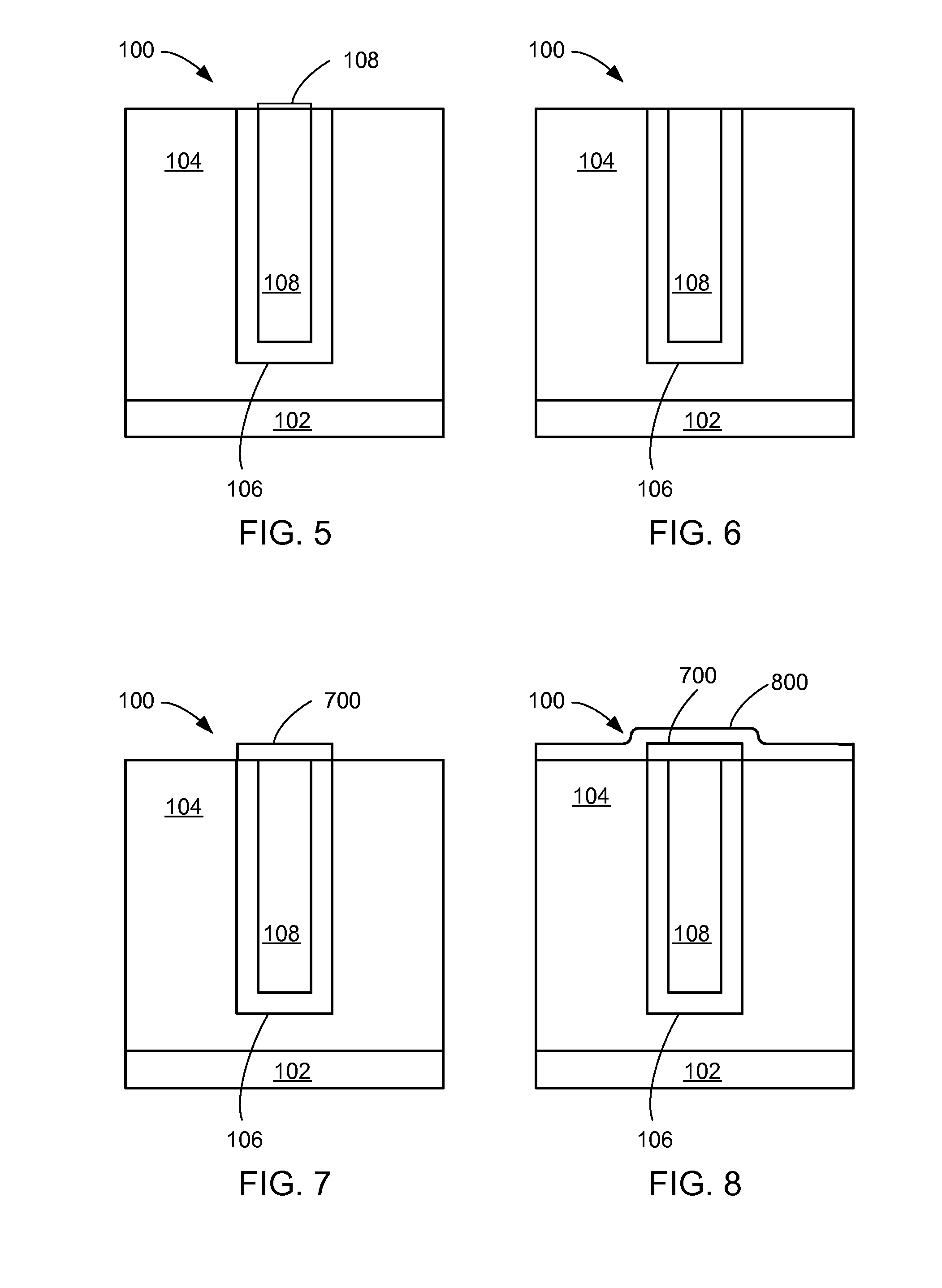
[0019]FIG. 5 is a close up view of the semiconductor interconnect after a CMP step according to a second embodiment of the present invention;
[0020]FIG. 6 is a close up view of the semiconductor interconnect after an
oxide removal step according to a second embodiment of the present invention;
[0021]FIG. 7 is a close up view of the semiconductor interconnect after a capping step according to a second embodiment of the present invention;
[0022]FIG. 8 is a close up view of the semiconductor interconnect after a post deposition treatment step according to a second embodiment of the present invention;
[0023]FIG. 9 is shown a semiconductor
system used in practicing an embodiment of the present invention; and
[0024]FIG. 10 is a
flow chart of a semiconductor system in accordance with another embodiment of the present invention.
[0025] The following embodiments are described in sufficient detail to enable those skilled in the art to make and use the invention. It is to be understood that other embodiments would be evident based on the present disclosure, and that system, process, or mechanical changes may be made without departing from the scope of the present invention.
[0026] In the following description, numerous specific details are given to provide a thorough understanding of the invention. However, it will be apparent that the invention may be practiced without these specific details. In order to avoid obscuring the present invention, some well-known circuits, system configurations, and process steps are not disclosed in detail.
[0027] Likewise, the drawings showing embodiments of the system are semi-diagrammatic and not to scale and, particularly, some of the dimensions are for the
clarity of presentation and are shown greatly exaggerated in the drawing FIGS.
[0028] In addition, where multiple embodiments are disclosed and described having some features in common, for
clarity and ease of illustration, description, and comprehension thereof, similar and like features one to another will ordinarily be described with like reference numerals. The embodiments have been numbered first embodiment, second embodiment, etc. as a matter of descriptive convenience and are not intended to have any other significance or provide limitations for the present invention.
[0029] For expository purposes, the term “horizontal” as used herein is defined as a
plane parallel to the plane or surface of the
integrated circuit, regardless of its orientation. The term “vertical” refers to a direction perpendicular to the horizontal as just defined. Terms, such as “above”, “below”, “bottom”, “top”, “side” (as in “sidewall”), “higher”, “lower”, “upper”, “over”, and “under”, are defined with respect to the horizontal plane. The term “on” means there is direct contact among elements.
[0030] The term “
processing” as used herein includes deposition of material, patterning,
exposure, development,
etching, cleaning, molding, and / or removal of the material or as required in forming a described structure.
[0031] The term “system” as used herein means and refers to the method and to the apparatus of the present invention in accordance with the context in which the term is used.
[0032] The present invention relates to fixing dielectric induced reliability problems by minimizing or eliminating ILD
contamination and surface degradation that results in higher leakage current, lower
voltage breakdown and shorter time-to-dielectric breakdown.
[0033] The process flow to form a capping layer on Cu interconnects is generally made up of several steps, which may include the following:
[0034] cleaning copper surface to establish a surface free from
copper oxide and strongly bound organic compounds; the same process step also serves to remove contaminants from the
dielectric surface;
[0035] rinsing off the cleaning chemicals from the
wafer surface;
[0037] post-treatment of the metal /
metal alloy cap and / or ILD to minimize deposition-induced ILD
contamination and / or promote
corrosion resistance of the film;
[0038] rinsing the
wafer surface with deionized water; and / or
[0040] Embodiments of the present invention generally add process steps at a given point into the process flow described above.
[0042] Spin rinse / dry technology that is used immediately after selectively depositing capping layer(s) on copper interconnects is not able to remove the
moisture completely. A significant reduction of
moisture can be achieved with one of the following processes:
[0044] i. baking in
inert (N2 etc.) environment or vacuum environment or
[0046] Both of the above are performed at a temperature of about 30° C. to about 150° C.
[0048] c.
drying with de-hydrated agent(s) such as but not limited to dehydrated
alcohol, performed after metal cap layer deposition; or
CH3COOCOCH3+H2O=2CH3COOH [0051] A further
advantage of these starting chemicals is that their reaction products are either gaseous or volatile compounds.
CH3COOCOCH3+H2O=2CH3COOH [0051] A further
advantage of these starting chemicals is that their reaction products are either gaseous or volatile compounds.
[0052] This process is implemented in the final drying part of the full metal cap layer
deposition process sequence. More specifically, after the metal / metal
alloy cap
deposition process, the
wafer is generally post-cleaned by simple chemical rinse or the chemical rinse in combination with scrub then rinsed again with or without chemicals in DI, then the wafer is spin-dried to remove non-adherent water. It is after this stage when the
water reactive chemical is introduced onto the wafer. After distributing the
water reactive liquid on the entire wafer surface and after proper reaction time the wafer is spin-dried and the process is finished. The reaction of the water reactive liquid can be performed at room or elevated temperature to change reaction time and reaction yield.
[0053] These processes are applied as a very last step, i.e. drying, in the process flow.
[0054] 2. Surface
contamination removal immediately after forming metal or metal
alloy cap on Cu structures:
[0055] a. by
plasma (e.g. Ar, N2, NH3, H2 . . . ) clean introduced after dying step in the process flow;
[0056] b. supercritical CO2 drying as the last step in the process sequence;
[0058] i. complexation (forming bonds in an
exothermic process using chemicals such as hydroxyethylethylenediaminetetraacetic acid (HEDTA),
cyanide, etc.) or
[0059] ii. altering the charge of the metal compound on ILD surface as well as the
surface charge of the ILD (i.e., low pH solution (pH<2) makes both the surface as well as the metal compound positively charged; the latter is achieved by decomposing the metal compound / complex by protonating the compound that is attached to the metal
ion;
[0060] d. dissolving metal if formed on the ILD in low pH solution;
[0055] a. by
plasma (e.g. Ar, N2, NH3, H2 . . . ) clean introduced after dying step in the process flow;
[0063] g. combination of any of the above with mechanically enhanced cleaning (e.g. scrub).
[0065] Processes c, d, and e are also included in the post-treatment phase of the capping process.
[0066] 3.
Surface modification by hydrophobic layer(s). Immediately prior (on ILD) to or after (ILD, metal cap, or both) the formation of metal or metal alloy cap on Cu structures. This hydrophobic layer could either selectively chemisorb on the dielectric, on the metal / metal alloy cap or cover both metallic capping layer (like CoWP, CoWB etc.) and
dielectric surface.
[0067] Such hydrophobic
layers can be formed using, but not limited to,
silanes containing at least one apolar group which is retained on the surface after bonding the
silane through another functionality to the substrate or other inorganic anions that are attached to hydrophobic group or groups, i.e. long
alkyl or
aryl chains. The reactive functional groups on the
silanes can be but not limited to Si—OR, Si—X or Si—NH—Si (where R is
alkyl or
aryl group and X is
halogen).
[0072] The layer can be formed by exposing the substrate to
silane vapors (for the volatile
silanes) or solvents, such as but not limited to ethyl
alcohol, i-
propanol, 1-methyl-2-pyrrolidinone or
chloroform, containing the most
moisture sensitive silanes or
aqueous solution for less
hydrolysis sensitive silanes as well as alkylphosphonates and alkylphosphates. The latter compounds, such as the less
hydrolysis sensitive silanes as well as alkylphosphonates and alkylphosphates, however, can also be applied in non-aqueous solutions.
[0070] When used as prior to the capping process (i.e. prior the formation of metal or metal alloy cap on Cu structures) both the ILD as well as the embedded Cu structures has to be cleaned. The cleaning should preferably remove
copper oxide from the copper structure in order to avoid
silane layer formation on Cu structure. Since silane attachment to
oxide-free copper is weak (if the silane compound does not contain strongly bonding groups such as amines, thiols etc.) the silane layer formation will be restricted to the dielectric area.
[0071] This process creates a hydrophobic layer, so the use of any functional groups going through
protonation /
deprotonation reaction or
hydrogen bonding in water is not recommended. Preferred water insensitive functionalities are alkyl, aryl, or their derivatives where one or more (or ultimately all) hydrogen atoms are exchanged to
halogen atoms such as
fluorine,
chlorine,
bromine,
iodine with fluorine being the most preferred.
[0072] The layer can be formed by exposing the substrate to silane vapors (for the volatile silanes) or solvents, such as but not limited to ethyl
alcohol, i-
propanol, 1-methyl-2-pyrrolidinone or
chloroform, containing the most moisture sensitive silanes or
aqueous solution for less
hydrolysis sensitive silanes as well as alkylphosphonates and alkylphosphates. The latter compounds, such as the less hydrolysis sensitive silanes as well as alkylphosphonates and alkylphosphates, however, can also be applied in non-aqueous solutions.
[0073] In addition the substrate can be exposed directly to the silane compound without using any
solvent if needed. The
exposure is preferably performed at
room temperature but lower or higher temperatures can also be used to control thickness and cross linking of the layer. Table 1 shows the results obtained with silane treatment on different type of dielectrics. TABLE 1
Contact angle (°)HydrophobicSubstrateNo processFull processlayer / full processSiO221<996Black
diamond391692
[0074] The hydrophobic
layers formed from the above detailed process also act as barriers against post-process moisture uptake. Such moisture uptake for instance during storage can induce oxidation and corrosion of capping layer, which ultimately leads to higher ILD contamination and consequently higher leakage current, worse voltage breakdown, and reduced TDDB performance. In addition, the barrier performance of the capping layer against
diffusion will also be adversely affected by corrosion.
[0075] The hydrophobic layer as outlined above can be formed prior to the actual capping layer deposition, right after the capping layer formation (see below) or as a part of post-treatment.
[0076] 4.
Surface modification by including the hydrophobic layer forming component into the deposition solution bath.
[0077] Any combination of the above mentioned methods is practical. The application is discussed with Cu interconnect as an example but not limited to Cu interconnect.
[0078] A patterned wafer is exposed to cleaning solution to remove
copper oxide from the surface then rinsed and dried. Subsequently, the wafer is exposed to
toluene trimethoxy silane vapor for 300 seconds at
room temperature, followed by i-
propanol and DI rinse. After these steps, the wafer either undergoes further cleaning step(s) or subjected to
electroless deposition followed by post-clean, if needed, then rinse and dry. The surface obtained in this manner retains a strongly hydrophobic character even after the entire
deposition process. In most cases, the
contact angle of the surface is higher after the full process with silane treatment than the non-processed wafer. In the absence of silane treatment, the
contact angle is significantly lower than that of the non-processed wafer. This statement is valid for
silicon oxide or other
silicon oxide containing dielectric materials such as Black
Diamond.
[0079] Referring now to FIG. 1, therein is shown a close up view of a semiconductor interconnect 100 after a CMP step according to a first embodiment of the present invention.
[0080] A semiconductor wafer 102 may be of a material such as silicon,
gallium arsenide,
diamond, etc. The semiconductor wafer 102 has been processed to form semiconductor elements, such as transistors, in and above it.
[0081] A dielectric layer 104, such as an ILD, has been deposited on the semiconductor wafer 102. The dielectric layer 104 is of dielectric materials such as
silicon oxide (SiOx), tetraethoxysilane (TEOS), borophosphosilicate (BPSG) glass, etc. with dielectric constants from 4.2 to 3.9 or low dielectric constant dielectric materials such as fluorinated tetraethoxysilane (FTEOS),
hydrogen silsesquioxane (HSQ),
benzocyclobutene (BCB), etc. with dielectric constants below 3.9. Ultra-low dielectric constant dielectric materials are dielectric materials having dielectric constants below 2.5. Examples of such materials include commercially available Teflon, Teflon-AF, Teflon
microemulsion, polimide nanofoams, silica aerogels, silica xerogels, and
mesoporous silica.

