[0016]These and / or other objects and advantages of the invention will become apparent and more readily appreciated from the following description of the preferred embodiments, taken in conjunction with the accompanying drawings of which:
[0017]FIG. 1 is a sectional view illustrating a embodiment of an organic light emitting display;
[0018]FIGS. 2A to 2C are sectional views illustrating a method of fabricating an organic light emitting display according to an embodiment;
[0019]FIG. 3A illustrates an organic light emitting display according to an embodiment;
[0020]FIG. 3B illustrates an organic light emitting display according to another embodiment; and
[0021]FIG. 3C illustrates an organic light emitting display according to another embodiment.
[0025]FIG. 4D is a cross-sectional view of the organic light emitting display of FIG. 4C, taken along the line d-d.
[0026]FIG. 4E is a schematic perspective view illustrating
mass production of organic light emitting devices in accordance with one embodiment.
[0027]Hereinafter, preferable embodiments according to the present invention will be described with reference to the attached drawings.
[0028]An organic light emitting display (OLED) is a display device comprising an array of organic light emitting diodes. Organic light emitting diodes are
solid state devices which include an organic material and are adapted to generate and emit light when appropriate electrical potentials are applied.
[0029]OLEDs can be generally grouped into two basic types dependent on the arrangement with which the stimulating
electrical current is provided. FIG. 4A schematically illustrates an exploded view of a simplified structure of a passive
matrix type OLED 1000. FIG. 4B schematically illustrates a simplified structure of an
active matrix type OLED 1001. In both configurations, the OLED 1000, 1001 includes OLED pixels built over a substrate 1002, and the OLED pixels include an
anode 1004, a
cathode 1006 and an
organic layer 1010. When an appropriate electrical potential is applied between the
anode 1004 and
cathode 1006, visible light is emitted from the
organic layer.
[0030]Referring to FIG. 4A, the passive matrix OLED (PMOLED) design includes elongate strips of
anode 1004 arranged generally perpendicular to elongate strips of
cathode 1006 with organic
layers interposed therebetween. The intersections of the strips of cathode 1006 and anode 1004 define individual OLED pixels where light is generated and emitted upon appropriate excitation of the corresponding strips of anode 1004 and cathode 1006. PMOLEDs provide the
advantage of relatively simple fabrication.
[0031]Referring to FIG. 4B, the active matrix OLED (
AMOLED) includes driving circuits 1012 arranged between the substrate 1002 and an array of OLED pixels. An individual pixel of AMOLEDs is defined between the common cathode 1006 and an anode 1004, which is electrically isolated from other anodes. Each
driving circuit 1012 is coupled with an anode 1004 of the OLED pixels and further coupled with a data line 1016 and a
scan line 1018. In embodiments, the scan lines 1018 supply select signals that select rows of the driving circuits, and the
data lines 1016 supply data signals for particular driving circuits. The data signals and scan signals stimulate the local driving circuits 1012, which excite the anodes 1004 so as to emit light from their corresponding pixels.
[0032]In the illustrated
AMOLED, the local driving circuits 1012, the
data lines 1016 and scan lines 1018 are buried in a planarization layer 1014, which is interposed between the
pixel array and the substrate 1002; The planarization layer 1014 provides a planar top surface on which the organic light emitting
pixel array is formed. The planarization layer 1014 may be formed of organic or
inorganic materials, and formed of two or more
layers although shown as a single layer. The local driving circuits 1012 are typically formed with thin film transistors (TFT) and arranged in a grid or array under the OLED
pixel array. The local driving circuits 1012 may be at least partly made of organic materials, including organic TFT.
[0033]AMOLEDs have the
advantage of fast refresh rates improving their desirability for use in displaying data signals. Also, AMOLEDs have the advantages of consuming less power than passive matrix OLEDs.
[0034]Referring to common features of the PMOLED and
AMOLED designs, the substrate 1002 provides structural support for the OLED pixels and circuits. In various embodiments, the substrate 1002 can comprise rigid or flexible materials as well as opaque or transparent materials, such as plastic, glass, and / or foil. As noted above, each OLED pixel or
diode is formed with the anode 1004, cathode 1006 and
organic layer 1010 interposed therebetween. When an appropriate electrical potential is applied between the anode 1004 and cathode 1006, the cathode 1006 injects electrons and the anode 1004 injects holes. In certain embodiments, the anode 1004 and cathode 1006 are inverted; i.e., the cathode is formed on the substrate 1002 and the anode is opposingly arranged.
[0035]Interposed between the cathode 1006 and anode 1004 are one or more organic
layers. More specifically, at least one emissive or light emitting layer is interposed between the cathode 1006 and anode 1004. The light emitting layer may comprise one or more light emitting organic compounds. Typically, the light emitting layer is configured to emit visible light in a single color such as blue, green or red. In the illustrated embodiment, one organic layer 1010 is formed between the cathode 1006 and anode 1004 and acts as a light emitting layer. Additional layers, which can be formed between the anode 1004 and cathode 1006, can include a hole transporting layer, a
hole injection layer, an
electron transporting layer and an
electron injection layer.
[0036]Hole transporting and / or injection layers can be interposed between the light emitting layer 1010 and the anode 1004.
Electron transporting and / or injecting layers can be interposed between the cathode 1006 and the light emitting layer 1010. The
electron injection layer facilitates injection of electrons from the cathode 1006 toward the light emitting layer 1010 by reducing the
work function for injecting electrons from the cathode 1006. Similarly, the
hole injection layer facilitates injection of holes from the anode 1004 toward the light emitting layer 1010. The hole and electron transporting layers facilitate movement of the carriers injected from the respective electrodes toward the light emitting layer.
[0037]In some embodiments, a single layer may serve both
electron injection and transportation functions or both hole injection and transportation functions. In some embodiments, one or more of these layers are lacking. In some embodiments, one or more organic layers are doped with one or more materials that help injection and / or transportation of the carriers. In embodiments where only one organic layer is formed between the cathode and anode, the organic layer may include not only an organic light emitting compound but also certain functional materials that help injection or transportation of carriers within that layer.
[0038]There are numerous organic materials that have been developed for use in these layers including the light emitting layer. Also, numerous other organic materials for use in these layers are being developed. In some embodiments, these organic materials may be macromolecules including oligomers and polymers. In some embodiments, the organic materials for these layers may be relatively small molecules. The skilled artisan will be able to select appropriate materials for each of these layers in view of the desired functions of the individual layers and the materials for the neighboring layers in particular designs.
[0039]In operation, an electrical circuit provides appropriate potential between the cathode 1006 and anode 1004. This results in an
electrical current flowing from the anode 1004 to the cathode 1006 via the interposed organic layer(s). In one embodiment, the cathode 1006 provides electrons to the adjacent organic layer 1010. The anode 1004 injects holes to the organic layer 1010. The holes and electrons recombine in the organic layer 1010 and generate energy particles called “excitons.” The excitons transfer their energy to the organic light emitting material in the organic layer 1010, and the energy is used to emit visible light from the organic light emitting material. The spectral characteristics of light generated and emitted by the OLED 1000, 1001 depend on the nature and composition of
organic molecules in the organic layer(s). The composition of the one or more organic layers can be selected to suit the needs of a particular application by one of ordinary skill in the art.
[0040]OLED devices can also be categorized based on the direction of the
light emission. In one type referred to as “top emission” type, OLED devices emit light and display images through the cathode or top
electrode 1006. In these embodiments, the cathode 1006 is made of a material transparent or at least partially transparent with respect to visible light. In certain embodiments, to avoid losing any light that can pass through the anode or bottom
electrode 1004, the anode may be made of a material substantially reflective of the visible light. A second type of OLED devices emits light through the anode or bottom
electrode 1004 and is called “bottom emission” type. In the bottom emission type OLED devices, the anode 1004 is made of a material which is at least partially transparent with respect to visible light. Often, in bottom emission type OLED devices, the cathode 1006 is made of a material substantially reflective of the visible light. A third type of OLED devices emits light in two directions, e.g. through both anode 1004 and cathode 1006. Depending upon the direction(s) of the
light emission, the substrate may be formed of a material which is transparent, opaque or reflective of visible light.
[0041]In many embodiments, an OLED pixel array 1021 comprising a plurality of organic light emitting pixels is arranged over a substrate 1002 as shown in FIG. 4C. In embodiments, the pixels in the array 1021 are controlled to be turned on and off by a
driving circuit (not shown), and the plurality of the pixels as a whole displays information or image on the array 1021. In certain embodiments, the OLED pixel array 1021 is arranged with respect to other components, such as drive and
control electronics to define a display region and a non-display region. In these embodiments, the display region refers to the area of the substrate 1002 where OLED pixel array 1021 is formed. The non-display region refers to the remaining areas of the substrate 1002. In embodiments, the non-display region can contain logic and / or power supply circuitry. It will be understood that there will be at least portions of control / drive circuit elements arranged within the display region. For example, in PMOLEDs, conductive components will extend into the display region to provide appropriate potential to the anode and cathodes. In AMOLEDs, local driving circuits and data / scan lines coupled with the driving circuits will extend into the display region to drive and control the individual pixels of the AMOLEDs.
[0042]One design and fabrication consideration in OLED devices is that certain organic material layers of OLED devices can suffer damage or accelerated deterioration from
exposure to water,
oxygen or other harmful gases. Accordingly, it is generally understood that OLED devices be sealed or encapsulated to inhibit
exposure to
moisture and
oxygen or other harmful gases found in a manufacturing or operational environment. FIG. 4D schematically illustrates a cross-section of an encapsulated OLED device 1011 having a
layout of FIG. 4C and taken along the line d-d of FIG. 4C. In this embodiment, a generally planar top plate or substrate 1061 engages with a seal 1071 which further engages with a bottom plate or substrate 1002 to enclose or encapsulate the OLED pixel array 1021. In other embodiments, one or more layers are formed on the top plate 1061 or bottom plate 1002, and the seal 1071 is coupled with the bottom or top substrate 1002, 1061 via such a layer. In the illustrated embodiment, the seal 1071 extends along the periphery of the OLED pixel array 1021 or the bottom or top plate 1002, 1061.
[0043]In embodiments, the seal 1071 is made of a frit material as will be further discussed below. In various embodiments, the top and bottom plates 1061, 1002 comprise materials such as plastics, glass and / or
metal foils which can provide a barrier to passage of
oxygen and / or water to thereby protect the OLED pixel array 1021 from
exposure to these substances. In embodiments, at least one of the top plate 1061 and the bottom plate 1002 are formed of a substantially transparent material.
[0044]To lengthen the
life time of OLED devices 1011, it is generally desired that seal 1071 and the top and bottom plates 1061, 1002 provide a substantially non-permeable seal to oxygen and
water vapor and provide a substantially hermetically enclosed space 1081. In certain applications, it is indicated that the seal 1071 of a frit material in combination with the top and bottom plates 1061, 1002 provide a barrier to oxygen of less than approximately 10−3 cc / m2-day and to water of less than 10−6 g / m2-day. Given that some oxygen and
moisture can permeate into the enclosed space 1081, in some embodiments, a material that can take up oxygen and / or
moisture is formed within the enclosed space 1081.
[0045]The seal 1071 has a width W, which is its thickness in a direction parallel to a surface of the top or bottom substrate 1061, 1002 as shown in FIG. 4D. The width varies among embodiments and ranges from about 300 μm to about 3000 μm, optionally from about 500 μm to about 1500 μm. Also, the width may vary at different positions of the seal 1071. In some embodiments, the width of the seal 1071 may be the largest where the seal 1071 contacts one of the bottom and top substrate 1002, 1061 or a layer formed thereon. The width may be the smallest where the seal 1071 contacts the other. The width variation in a single cross-section of the seal 1071 relates to the cross-sectional shape of the seal 1071 and other design parameters.
[0046]The seal 1071 has a height H, which is its thickness in a direction perpendicular to a surface of the top or bottom substrate 1061, 1002 as shown in FIG. 4D. The height varies among embodiments and ranges from about 2 μm to about 30 μm, optionally from about 10 μm to about 15 μm. Generally, the height does not significantly vary at different positions of the seal 1071. However, in certain embodiments, the height of the seal 1071 may vary at different positions thereof
[0047]In the illustrated embodiment, the seal 1071 has a generally rectangular cross-section. In other embodiments, however, the seal 1071 can have other various cross-sectional shapes such as a generally square cross-section, a generally trapezoidal cross-section, a cross-section with one or more rounded edges, or other configuration as indicated by the needs of a given application. To improve hermeticity, it is generally desired to increase the interfacial area where the seal 1071 directly contacts the bottom or top substrate 1002, 1061 or a layer formed thereon. In some embodiments, the shape of the seal can be designed such that the interfacial area can be increased.
[0048]The seal 1071 can be arranged immediately adjacent the OLED array 1021, and in other embodiments, the seal 1071 is spaced some distance from the OLED array 1021. In certain embodiment, the seal 1071 comprises generally linear segments that are connected together to surround the OLED array 1021. Such linear segments of the seal 1071 can extend, in certain embodiments, generally parallel to respective boundaries of the OLED array 1021. In other embodiment, one or more of the linear segments of the seal 1071 are arranged in a non-parallel relationship with respective boundaries of the OLED array 1021. In yet other embodiments, at least part of the seal 1071 extends between the top plate 1061 and bottom plate 1002 in a curvilinear manner.
[0049]As noted above, in certain embodiments, the seal 1071 is formed using a frit material or simply “frit” or glass frit,” which includes fine glass particles. The frit particles includes one or more of
magnesium oxide (MgO),
calcium oxide (CaO),
barium oxide (BaO),
lithium oxide (Li2O),
sodium oxide (Na2O),
potassium oxide (K2O),
boron oxide (B2O3),
vanadium oxide (V2O5),
zinc oxide (ZnO),
tellurium oxide (TeO2), aluminum oxide (Al2O3),
silicon dioxide (SiO2),
lead oxide (PbO),
tin oxide (SnO), phosphorous oxide (P2O5),
ruthenium oxide (Ru2O),
rubidium oxide (Rb2O),
rhodium oxide (Rh2O), ferrite oxide (Fe2O3),
copper oxide (CuO),
titanium oxide (TiO2),
tungsten oxide (WO3),
bismuth oxide (Bi2O3),
antimony oxide (Sb2O3), lead-
borate glass,
tin-
phosphate glass,
vanadate glass, and borosilicate, etc. In embodiments, these particles range in size from about 2 μm to about 30 μm, optionally about 5 μm to about 10 μm, although not limited only thereto. The particles can be as large as about the distance between the top and bottom substrates 1061, 1002 or any layers formed on these substrates where the frit seal 1071 contacts.
[0050]The frit material used to form the seal 1071 can also include one or more filler or additive materials. The filler or additive materials can be provided to adjust an overall
thermal expansion characteristic of the seal 1071 and / or to adjust the absorption characteristics of the seal 1071 for selected frequencies of incident
radiant energy. The filler or additive material(s) can also include inversion and / or additive fillers to adjust a coefficient of
thermal expansion of the frit. For example, the filler or additive materials can include transition metals, such as
chromium (Cr), iron (Fe),
manganese (Mn),
cobalt (Co),
copper (Cu), and / or
vanadium. Additional materials for the filler or additives include ZnSiO4, PbTiO3, ZrO2, eucryptite.
[0051]In embodiments, a frit material as a dry composition contains glass particles from about 20 to 90 about wt %, and the remaining includes fillers and / or additives. In some embodiments, the frit paste contains about 10-30 wt % organic materials and about 70-90%
inorganic materials. In some embodiments, the frit paste contains about 20 wt % organic materials and about 80 wt %
inorganic materials. In some embodiments, the organic materials may include about 0-30 wt % binder(s) and about 70-100 wt %
solvent(s). In some embodiments, about 10 wt % is binder(s) and about 90 wt % is
solvent(s) among the organic materials. In some embodiments, the inorganic materials may include about 0-10 wt % additives, about 20-40 wt % fillers and about 50-80 wt % glass
powder. In some embodiments, about 0-5 wt % is additive(s), about 25-30 wt % is filler(s) and about 65-75 wt % is the glass
powder among the inorganic materials.
[0052]In forming a ftit seal, a liquid material is added to the dry frit material to form a frit paste. Any organic or
inorganic solvent with or without additives can be used as the liquid material. In embodiments, the
solvent includes one or more organic compounds. For example, applicable organic compounds are
ethyl cellulose, nitro
cellulose, hydroxyl propyl
cellulose,
butyl carbitol acetate,
terpineol, butyl cellusolve,
acrylate compounds. Then, the thus formed frit paste can be applied to form a shape of the seal 1071 on the top and / or bottom plate 1061, 1002.
[0053]In one exemplary embodiment, a shape of the seal 1071 is initially formed from the frit paste and interposed between the top plate 1061 and the bottom plate 1002. The seal 1071 can in certain embodiments be pre-cured or pre-sintered to one of the top plate and bottom plate 1061, 1002. Following
assembly of the top plate 1061 and the bottom plate 1002 with the seal 1071 interposed therebetween, portions of the seal 1071 are selectively heated such that the frit material forming the seal 1071 at least partially melts. The seal 1071 is then allowed to resolidify to form a secure joint between the top plate 1061 and the bottom plate 1002 to thereby inhibit exposure of the enclosed OLED pixel array 1021 to oxygen or water.
[0054]In embodiments, the selective heating of the frit seal is carried out by
irradiation of light, such as a
laser or directed
infrared lamp. As previously noted, the frit material forming the seal 1071 can be combined with one or more additives or filler such as species selected for improved absorption of the irradiated light to facilitate heating and melting of the frit material to form the seal 1071.
[0055]In some embodiments, OLED devices 1011 are
mass produced. In an embodiment illustrated in FIG. 4E, a plurality of separate OLED arrays 1021 is formed on a common bottom substrate 1101. In the illustrated embodiment, each OLED array 1021 is surrounded by a shaped frit to form the seal 1071. In embodiments, common top substrate (not shown) is placed over the common bottom substrate 1101 and the structures formed thereon such that the OLED arrays 1021 and the shaped frit paste are interposed between the common bottom substrate 1101 and the common top substrate. The OLED arrays 1021 are encapsulated and sealed, such as via the previously described
enclosure process for a single OLED display device. The resulting product includes a plurality of OLED devices kept together by the common bottom and top substrates. Then, the resulting product is
cut into a plurality of pieces, each of which constitutes an OLED device 1011 of FIG. 4D. In certain embodiments, the individual OLED devices 1011 then further undergo additional packaging operations to further improve the sealing formed by the frit seal 1071 and the top and bottom substrates 1061, 1002.
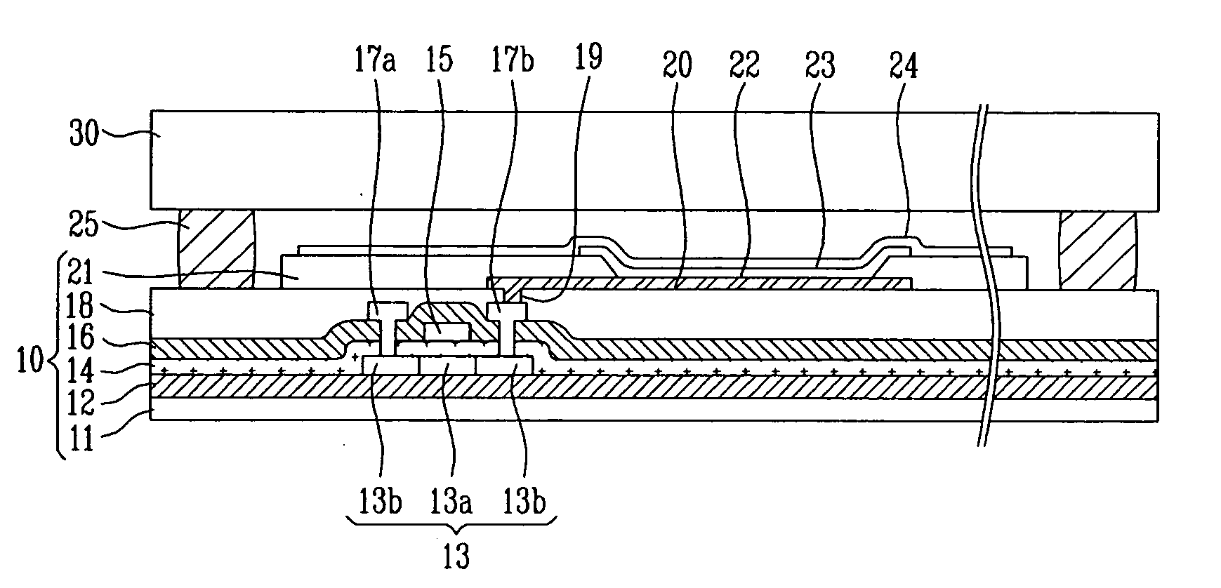
[0056]FIG. 1 is a sectional view illustrating an organic light emitting display. Referring to FIG. 1, the organic light emitting display includes a first substrate 10, a frit 25, and a second substrate 30. The first substrate 10 including a deposition substrate 11 and at least one organic
light emitting diode including a first electrode 20, an organic layer 22, and a second electrode 23 formed above the deposition substrate 11. First, a buffer layer 12 is formed on the deposition substrate 11. The deposition substrate 11 may comprise glass and the buffer layer is formed of an insulating material such as SiO2 and SiNx. The buffer layer 12 is formed to prevent the deposition substrate 11 from being damaged by factors such as heat from the outside.
[0057]A
semiconductor layer 13, including an
active layer 13a and source and drain regions 13b is formed on at least one region of the buffer layer 12. A gate insulating layer 14 is formed on the buffer layer 12 to cover the
semiconductor layer 13. A gate electrode 15 of similar size to the
active layer 13a is formed on one region of the gate insulating layer 14.
[0058]An interlayer
insulation layer 16 is formed on the gate insulating layer 14 to include the gate electrode 15. Source and drain electrodes 17a and 17b are formed on a predetermined region of the interlayer
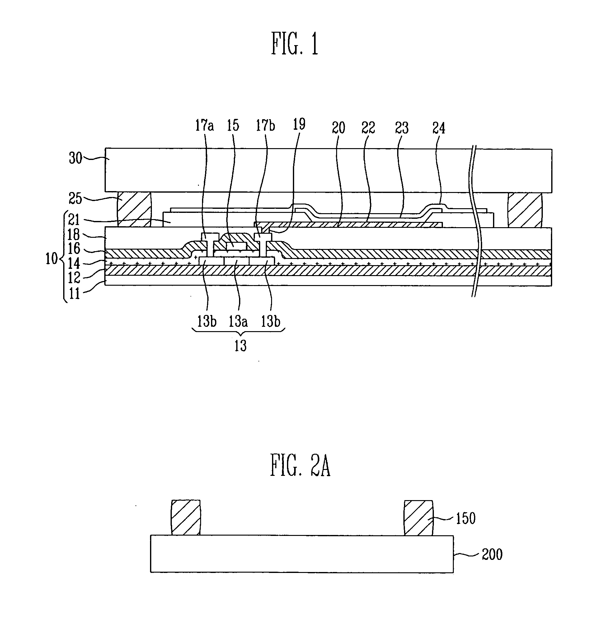
insulation layer 16 so as to contact the source and drain regions 13b of the
semiconductor layer 13.
[0059]A planarization layer 18 is formed on the interlayer
insulation layer 16 to include the source and drain electrodes 17a and 17b. The first electrode 20 is formed on one region of the planarization layer 18. At this time, the first electrode 20 is connected to one exposed region of one of the source and drain electrodes 17a and 17b by a via hole 19.
[0060]A pixel definition layer 21, including an aperture that exposes at least one region of the first electrode 20, is formed on the planarization layer 18 to include the first electrode 20. An organic layer 22 is formed on the aperture of the pixel definition layer 21 and a second electrode layer 23 is formed on the pixel definition layer 21 to include the organic layer 22. A frit 25 is provided between a non-pixel region of the first substrate 10 and the second substrate 30 to adhere the first substrate 10 and the second substrate 30 to each other.
[0061]FIGS. 2A to 2C are sectional views illustrating a method of fabricating an organic light emitting display according to an embodiment. The organic light emitting display includes a first substrate 100 including a pixel region (not shown) in which at least one organic light emitting display device (OLED) 110 is formed. A non-pixel region (not shown) surrounds the pixel region. A second substrate 200 is attached to a portion of the non-pixel region of the first substrate 100 with a frit 150. According to a first method of fabricating the organic light emitting display, the frit 150 is applied on one region of the second substrate 200 such that the frit 150 is interposed between the second substrate 200 and the non-pixel region of the first substrate 100. In some embodiments, the frit 150 may include additives such as a filler material for controlling a
thermal expansion coefficient and / or an
absorbent material that absorbs
laser or
infrared rays.
[0062]In some embodiments, the frit 150 may be formed using a screen-printing method. According to the
screen printing method, a desired pattern is designed to be drawn on a
metal sheet, the portion of the
metal sheet excluding the pattern is masked using an
emulsion solution, and the frit is applied such that the desired pattern is printed on the second substrate 200.
[0063]After the frit 150 is applied to the substrate 200, the frit 150 is annealed at a predetermined temperature. Due to the process of annealing the frit 150, an organic material added to the frit 150 to make the frit 150 a gel-type paste is extinguished in the air such that the frit 150 is hardened or solidified. The process of annealing the frit 150 is preferably performed in a furnace at a temperature between 300° C. and 700° C. (FIG. 2A).
[0064]Next, the first substrate 100 is provided to be attached to the second substrate 200. At this time, in order to seal up the organic
light emitting diode 110 formed on the first substrate 100, the first substrate 100 and the second substrate 200 are arranged such that the organic light emitting
diode 110 is located between the substrates 100 and 200 and surrounded by the frit 150. In the example shown in FIGS. 2B and 2C, a region of the non-pixel region on the first substrate 100 includes non-planar structures formed on the surface where the frit contacts the substrate 100. The non-planar structures comprise one or more valleys and peaks, or other forms of three-dimensional geography, and serve to increase the contact surface area of an integrating interface where the frit 150 and the first substrate 100 are connected to each other. The increased contact surface area improves the
adhesive force provided by the frit 150 adhering the first substrate 100 to the second substrate 200. The surface contacted to the frit 150 of the first substrate 100 is preferably an
inorganic layer. When the frit 150 is directly contacted to an organic layer, the organic layer may be vulnerable to heat and may be damaged by high temperatures such as when a
laser beam is used to irradiate the frit 150. Therefore, the
adhesive force between the surface and the frit 150 may deteriorate. The process of making the non-planar structures on the exposed surface of the first substrate 100 may be performed by
etching, preferably,
dry etching. The
dry etching process may include methods such as
ion beam
etching, RF
sputtering etching, and
reactive ion etching.
[0065]After the substrates 100 and 200 are attached by the frit 150, the frit 150 is irradiated with a laser beam or
infrared rays to be melted such that the first substrate 100 and the second substrate 200 are adhered to each other. At this time, the preferable intensity of the laser beam for melting the frit 150 is in a range of about 20 W to about 60 W (FIG. 2C)
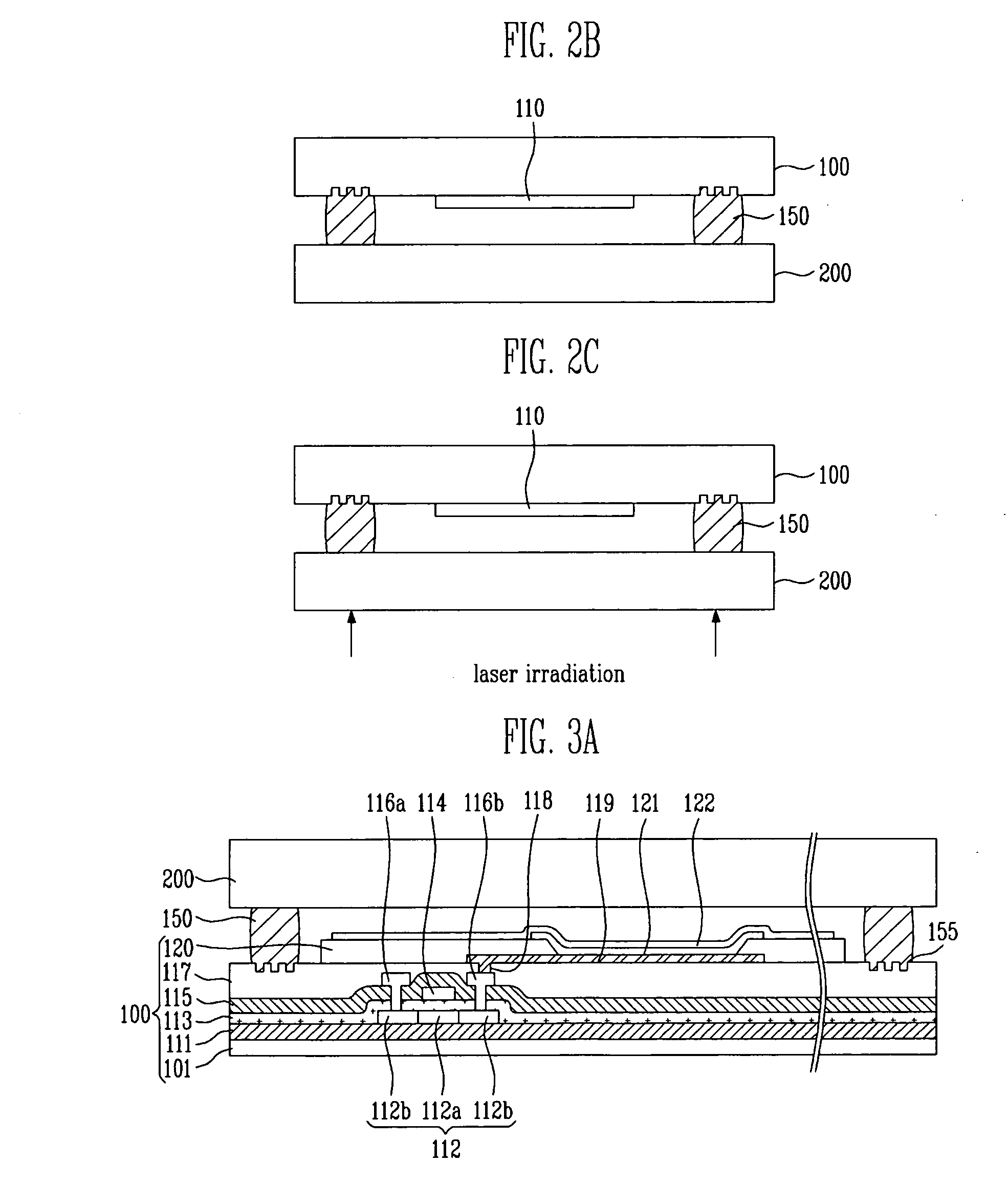
[0066]FIG. 3A illustrates an organic light emitting display according to an embodiment. Referring to FIG. 3A, the organic light emitting display includes the first substrate 100, the frit 150, and the second substrate 200.
[0067]The first substrate 100 includes a deposition substrate 101 and at least one organic light emitting
diode formed on the deposition substrate 101. First, a buffer layer 111 is formed on the deposition substrate 101. The deposition substrate 101 is formed of glass and the buffer layer 111 is formed of an insulating material such as SiO2 and SiNx. The buffer layer 111 is formed to prevent the deposition substrate 101 from being damaged by factors such as heat from the outside.
[0068]A semiconductor layer 112 including an
active layer 112a and source and drain regions 112b is formed on at least one region of the buffer layer 111. A gate insulation layer 113 is formed on the buffer layer 111 to cover the semiconductor layer 112. A gate electrode 114 of a similar size corresponding to the width of the active layer 112a is formed on one region of the gate insulation layer 113.
[0069]An interlayer insulation layer 115 is formed on the gate insulation layer 113 to include the gate electrode 114. Source and drain electrodes 116a and 116b are formed on a predetermined region of the interlayer insulation layer 115. Each of the source and drain electrodes 116a and 116b is connected to one exposed region of each of the source and drain regions 112b. A planarization layer 117 is formed on the interlayer insulation layer 115 to cover at least the source and drain electrodes 116a and 116b.
[0070]A first electrode 119 is formed on one region of the planarization layer 117 such that the first electrode layer 119 is connected to an exposed region of one of the source and drain electrodes 116a and 116b by a via hole 118. At this time, at least one non-planar structure 155 is formed in a portion of the the non-pixel region of the planarization layer 117. The non-planar structures comprise one or more valleys and peaks. The valleys and peaks of the non-planar structure 155 may be rectangular in cross section as shown in FIG. 3A, but this is only an example. The non-planar structures 155 may be of any regular or
irregular shape such as triangular, semicircular, smooth edged, sharp edged, undulating, etc.
[0071]At this time, since the planarization layer 117 is formed on the uppermost layer of the first substrate 100 to be adhered to the frit 150 and the surface including the non-planar structures 155 is directly contacted to the frit 150, the adhesive force between the frit 150 and the planarization layer 117 is stronger than if there were no non-planar structures. Therefore, the planarization layer 117 is made non-planar to increase the area in which the planarization layer 117 and the frit 150 are contacted to each other so that it is possible to improve the adhesive force afforded by the frit 150 between the first substrate 100 and the second substrate 200. The planarization layer 117 is preferably formed of an inorganic insulation layer. Thus, when a laser beam or infrared rays are used to irradiate the frit 150 to melt the frit 150, the
inorganic layer is insensitive to heat, and the organic light emitting diode is not damaged. The non-planar structures 155 may be formed in the planarazation layer by etching, preferably
dry etching. The dry etching may be performed methods such as
ion beam etching, RF
sputtering etching, and
reactive ion etching.

